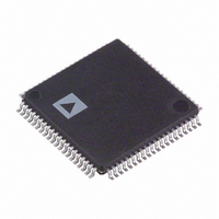
ADV7183BBSTZ Analog Devices Inc, ADV7183BBSTZ Datasheet - Page 14

ADV7183BBSTZ
Manufacturer Part Number
ADV7183BBSTZ
Description
IC,TV/VIDEO CIRCUIT,Color Decoder Circuit,CMOS,QFP,80PIN,PLASTIC
Manufacturer
Analog Devices Inc
Type
Video Decoderr
Datasheet
1.ADV7183BKSTZ.pdf
(100 pages)
Specifications of ADV7183BBSTZ
Applications
Projectors, Recorders, Security
Voltage - Supply, Analog
3.15 V ~ 3.45 V
Voltage - Supply, Digital
1.65 V ~ 2 V
Mounting Type
Surface Mount
Package / Case
80-LQFP
Lead Free Status / RoHS Status
Lead free / RoHS Compliant
Available stocks
Company
Part Number
Manufacturer
Quantity
Price
Company:
Part Number:
ADV7183BBSTZ
Manufacturer:
AD
Quantity:
670
Company:
Part Number:
ADV7183BBSTZ
Manufacturer:
Analog Devices Inc
Quantity:
10 000
ADV7183B
Table 8. Input Channel Switching Using INSEL[3:0]
INSEL[3:0]
0000 (default)
0001
0010
0011
0100
0101
0110
0111
1000
1001
1010
1011
1100
1101
1110
1111
Analog Input Pins
CVBS1 = AIN1
CVBS2 = AIN2
CVBS3 = AIN3
CVBS4 = AIN4
CVBS5 = AIN5
CVBS6 = AIN6
Y1 = AIN1
C1 = AIN4
Y2 = AIN2
C2 = AIN5
Y3 = AIN3
C3 = AIN6
Y1 = AIN1
PB1 = AIN4
PR1 = AIN5
Y2 = AIN2
PB2 = AIN3
PR2 = AIN6
CVBS7 = AIN7
CVBS8 = AIN8
CVBS9 = AIN9
CVBS10 = AIN10
CVBS11 = AIN11
SET INSEL[3:0] FOR REQUIRED
MUXING CONFIGURATION
Description
YES
Video Format
Composite
Composite
Composite
Composite
Composite
Composite
Y/C
Y/C
Y/C
Y/C
Y/C
Y/C
YPrPb
YPrPb
YPrPb
YPrPb
YPrPb
YPrPb
Composite
Composite
Composite
Composite
Composite
Figure 7. Input Muxing Overview
INPUT MUXING; SEE TABLE 9
ADI RECOMMENDED
Rev. B | Page 14 of 100
ANALOG SIGNALS
CONNECTING
TO ADV7183B
Table 9. Input Channel Assignments
Input
Channel
AIN7
AIN1
AIN8
AIN2
AIN9
AIN3
AIN10
AIN4
AIN11
AIN5
AIN12
AIN6
ADI recommended input muxing is designed to minimize
crosstalk between signal channels and to obtain the highest
level of signal integrity.
should connect analog video signals to the ADV7183B.
It is strongly recommended to connect any unused analog input
pins to AGND to act as a shield.
Inputs AIN7 to AIN11 should be connected to AGND when
only six input channels are used. This improves the quality of
the sampling due to better isolation between the channels.
AIN12 is not under the control of INSEL[3:0]. It can be routed
to ADC0/ADC1/ADC2 only by manual muxing. See
for details.
(ADC_SW_MAN_EN, ADC0_SW,
USE MANUAL INPUT MUXING
CONFIGURE ADV7183B TO
DECODE VIDEO FORMAT:
ADC1_SW, ADC2_SW)
SET INSEL[3:0] TO
NO
Pin
No.
41
42
43
44
45
46
57
58
59
60
61
62
YPrPb: 1001
CVBS: 0000
YC: 0110
CVBS7
CVBS1
CVBS8
CVBS2
CVBS9
CVBS3
CVBS10
CVBS4
CVBS11
CVBS5
Not available
CVBS6
ADI Recommended Input Muxing Control
T able 9 summarizes how the PCB layout
1 4 4 H
INSEL[3:0]
Y/C1-Y
Y/C2-Y
Y/C3-Y
Y/C1-C
Y/C2-C
Y/C3-C
YPrPb1-Y
YPrPb2-Y
YPrPb2-Pb
YPrPb1-Pb
YPrPb1-Pr
YPrPb2-Pr
T able 10
1 4 5 H


