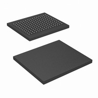
CY7C1423AV18-250BZC Cypress Semiconductor Corp, CY7C1423AV18-250BZC Datasheet - Page 12

CY7C1423AV18-250BZC
Manufacturer Part Number
CY7C1423AV18-250BZC
Description
SRAM (Static RAM)
Manufacturer
Cypress Semiconductor Corp
Datasheet
1.CY7C1423AV18-250BZC.pdf
(33 pages)
Specifications of CY7C1423AV18-250BZC
Format - Memory
RAM
Memory Type
SRAM - Synchronous, DDR II
Memory Size
36M (2M x 18)
Speed
250MHz
Interface
Parallel
Voltage - Supply
1.7 V ~ 1.9 V
Operating Temperature
0°C ~ 70°C
Package / Case
165-TFBGA
Density
36Mb
Access Time (max)
0.45ns
Sync/async
Synchronous
Architecture
DDR
Clock Freq (max)
250MHz
Operating Supply Voltage (typ)
1.8V
Address Bus
20b
Package Type
FBGA
Operating Temp Range
0C to 70C
Number Of Ports
2
Supply Current
740mA
Operating Supply Voltage (min)
1.7V
Operating Supply Voltage (max)
1.9V
Operating Temperature Classification
Commercial
Mounting
Surface Mount
Pin Count
165
Word Size
18b
Number Of Words
2M
Lead Free Status / RoHS Status
Contains lead / RoHS non-compliant
Lead Free Status / RoHS Status
Contains lead / RoHS non-compliant
Available stocks
Company
Part Number
Manufacturer
Quantity
Price
Company:
Part Number:
CY7C1423AV18-250BZC
Manufacturer:
Cypress Semiconductor Corp
Quantity:
10 000
Truth Table
The truth table for CY7C1422AV18, CY7C1429AV18, CY7C1423AV18, and CY7C1424AV18 follows.
Write Cycle Descriptions
The write cycle description table for CY7C1422AV18 and CY7C1423AV18 follows.
Notes
Document Number: 38-05617 Rev. *I
Write Cycle:
Load address; wait one cycle;
input write data on consecutive K and K rising edges.
Read Cycle:
Load address; wait one and a half cycle;
read data on consecutive C and C rising edges.
NOP: No Operation
Standby: Clock Stopped
2. X = “Don't Care,” H = Logic HIGH, L = Logic LOW,
3. Device powers up deselected with the outputs in a tri-state condition.
4. “A” represents address location latched by the devices when transaction was initiated. A + 0, A + 1 represents the internal address sequence in the burst.
5. “t” represents the cycle at which a Read/Write operation is started. t + 1, and t + 2 are the first, and second clock cycles respectively succeeding the “t” clock cycle.
6. Data inputs are registered at K and K rising edges. Data outputs are delivered on C and C rising edges, except when in single clock mode.
7. It is recommended that K = K and C = C = HIGH when clock is stopped. This is not essential, but permits most rapid restart by overcoming transmission line charging
8. Is based on a write cycle that was initiated in accordance with the
BWS
NWS
H
H
H
H
symmetrically.
different portions of a write cycle, as long as the setup and hold requirements are achieved.
L
L
L
L
0
0
/
BWS
NWS
H
H
H
H
L
L
L
L
1
1
/
L–H
L–H
L–H
L–H
K
–
–
–
–
Operation
L–H During the data portion of a write sequence
L–H During the data portion of a write sequence
L–H No data is written into the devices during this portion of a write operation.
L-H During the data portion of a write sequence
K
–
–
–
–
During the data portion of a write sequence
CY7C1422AV18 both nibbles (D
CY7C1423AV18 both bytes (D
CY7C1422AV18 both nibbles (D
CY7C1423AV18 both bytes (D
During the data portion of a write sequence
CY7C1422AV18 only the lower nibble (D
CY7C1423AV18 only the lower byte (D
CY7C1422AV18 only the lower nibble (D
CY7C1423AV18 only the lower byte (D
During the data portion of a write sequence
CY7C1422AV18 only the upper nibble (D
CY7C1423AV18 only the upper byte (D
CY7C1422AV18 only the upper nibble (D
CY7C1423AV18 only the upper byte (D
No data is written into the devices during this portion of a write operation.
represents rising edge.
Write Cycle Descriptions
Stopped
[17:0]
[17:0]
L-H
L-H
L-H
[7:0]
[7:0]
K
) are written into the device.
) are written into the device.
) are written into the device.
) are written into the device.
[8:0]
[8:0]
[17:9]
[17:9]
[3:0]
[3:0]
[7:4]
[7:4]
LD
table. NWS
H
X
L
L
Comments
) is written into the device, D
) is written into the device, D
) is written into the device, D
) is written into the device, D
) is written into the device, D
) is written into the device, D
) is written into the device, D
) is written into the device, D
CY7C1422AV18, CY7C1429AV18
CY7C1423AV18, CY7C1424AV18
R/W
H
X
X
L
[2, 8]
0
, NWS
D(A + 0) at K(t + 1) D(A + 1) at K(t + 1)
Q(A + 0) at C(t + 1) Q(A + 1) at C(t + 2)
High Z
Previous State
1
, BWS
0
DQ
, BWS
1
[2, 3, 4, 5, 6, 7]
, BWS
[17:9]
[17:9]
[8:0]
[8:0]
[7:4]
[7:4]
[3:0]
[3:0]
2
and BWS
remains unaltered.
remains unaltered.
remains unaltered.
remains unaltered.
High Z
Previous State
remains unaltered.
remains unaltered.
remains unaltered.
remains unaltered.
3
can be altered on
Page 12 of 33
DQ
[+] Feedback


