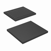
CY7C1423AV18-250BZC Cypress Semiconductor Corp, CY7C1423AV18-250BZC Datasheet - Page 24

CY7C1423AV18-250BZC
Manufacturer Part Number
CY7C1423AV18-250BZC
Description
SRAM (Static RAM)
Manufacturer
Cypress Semiconductor Corp
Datasheet
1.CY7C1423AV18-250BZC.pdf
(33 pages)
Specifications of CY7C1423AV18-250BZC
Format - Memory
RAM
Memory Type
SRAM - Synchronous, DDR II
Memory Size
36M (2M x 18)
Speed
250MHz
Interface
Parallel
Voltage - Supply
1.7 V ~ 1.9 V
Operating Temperature
0°C ~ 70°C
Package / Case
165-TFBGA
Density
36Mb
Access Time (max)
0.45ns
Sync/async
Synchronous
Architecture
DDR
Clock Freq (max)
250MHz
Operating Supply Voltage (typ)
1.8V
Address Bus
20b
Package Type
FBGA
Operating Temp Range
0C to 70C
Number Of Ports
2
Supply Current
740mA
Operating Supply Voltage (min)
1.7V
Operating Supply Voltage (max)
1.9V
Operating Temperature Classification
Commercial
Mounting
Surface Mount
Pin Count
165
Word Size
18b
Number Of Words
2M
Lead Free Status / RoHS Status
Contains lead / RoHS non-compliant
Lead Free Status / RoHS Status
Contains lead / RoHS non-compliant
Available stocks
Company
Part Number
Manufacturer
Quantity
Price
Company:
Part Number:
CY7C1423AV18-250BZC
Manufacturer:
Cypress Semiconductor Corp
Quantity:
10 000
Capacitance
Tested initially and after any design or process change that may affect these parameters.
Thermal Resistance
Tested initially and after any design or process change that may affect these parameters.
Note
Document Number: 38-05617 Rev. *I
C
C
C
26. Unless otherwise noted, test conditions are based on signal transition time of 2 V/ns, timing reference levels of 0.75 V, Vref = 0.75 V, RQ = 250 , V
Parameter
Parameter
IN
CLK
O
pulse levels of 0.25 V to 1.25 V, and output loading of the specified I
JA
JC
OUTPUT
Device
Under
Test
V
REF
ZQ
Input Capacitance
Clock Input Capacitance
Output Capacitance
Thermal Resistance
(Junction to Ambient)
Thermal Resistance
(Junction to Case)
(a)
Z
RQ =
250
0.75 V
0
= 50
Description
Description
V
REF
R
L
= 0.75 V
= 50
Figure 4. AC Test Loads and Waveforms
INCLUDING
T
Test conditions follow standard test methods and
procedures for measuring thermal impedance, in
accordance with EIA/JESD51.
Device
Under
Test
OUTPUT
A
JIG AND
SCOPE
= 25 C, f = 1 MHz, V
V
REF
ZQ
OL
/I
OH
and load capacitance shown in (a) of
0.75 V
RQ =
250
(b)
Test Conditions
Test Conditions
V
REF
= 0.75 V
DD
R = 50
5 pF
= 1.8 V, V
CY7C1422AV18, CY7C1429AV18
CY7C1423AV18, CY7C1424AV18
0.25 V
DDQ
= 1.5 V
AC Test Loads and
1.25 V
Slew Rate = 2 V/ns
ALL INPUT PULSES
0.75 V
165 FBGA
Package
Max
17.2
3.2
Waveforms.
5
4
5
[26]
DDQ
Page 24 of 33
°C/W
°C/W
= 1.5 V, input
Unit
Unit
pF
pF
pF
[+] Feedback


