BAT54SWT1G ON Semiconductor, BAT54SWT1G Datasheet

DIODE SCHOTTKY DUAL 30V SOT323

BAT54SWT1G

Manufacturer Part Number
BAT54SWT1G
Description
DIODE SCHOTTKY DUAL 30V SOT323
Manufacturer
ON Semiconductor
Datasheets

Specifications of BAT54SWT1G

Voltage - Forward (vf) (max) @ If
800mV @ 100mA
Current - Reverse Leakage @ Vr
2µA @ 25V
Current - Average Rectified (io) (per Diode)
200mA (DC)
Voltage - Dc Reverse (vr) (max)
30V
Reverse Recovery Time (trr)
5ns
Diode Type
Schottky
Speed
Small Signal =< 200mA (Io), Any Speed
Diode Configuration
1 Pair Series Connection
Mounting Type
Surface Mount
Package / Case
SC-70-3, SOT-323-3
Product
Schottky Diodes
Peak Reverse Voltage
30 V
Forward Continuous Current
0.2 A
Max Surge Current
0.6 A
Configuration
Dual Series
Recovery Time
5 ns
Forward Voltage Drop
0.8 V @ 0.1 A
Maximum Reverse Leakage Current
2 uA @ 25 V
Operating Temperature Range
- 55 C to + 125 C
Mounting Style
SMD/SMT
Current, Forward
200 mA
Package Type
SOT-323 (SC-70)
Power Dissipation
200 mW
Primary Type
Schottky Barrier
Speed, Switching
Fast
Temperature, Junction, Maximum
+125 °C
Temperature, Operating
-55 to +125 °C
Time, Recovery
5 ns
Voltage, Forward
0.52 V
Voltage, Reverse
30 V
Lead Free Status / RoHS Status
Lead free / RoHS Compliant
Other names
BAT54SWT1GOSTR

Available stocks

Company
Part Number
Manufacturer
Quantity
Price
Part Number:
BAT54SWT1G
Manufacturer:
ON Semiconductor
Quantity:
114 811
Part Number:
BAT54SWT1G
Manufacturer:
ON Semiconductor
Quantity:
16 650
Part Number:
BAT54SWT1G
Manufacturer:
ON/安森美
Quantity:
20 000
Company:
Part Number:
BAT54SWT1G
Quantity:
24 000
BAT54SWT1G
Dual Series Schottky
Barrier Diodes
applications, circuit protection, and voltage clamping. Extremely low
forward voltage reduces conduction loss. Miniature surface mount
package is excellent for hand held and portable applications where
space is limited.
Features
Stresses exceeding Maximum Ratings may damage the device. Maximum
Ratings are stress ratings only. Functional operation above the Recommended
Operating Conditions is not implied. Extended exposure to stresses above the
Recommended Operating Conditions may affect device reliability.
© Semiconductor Components Industries, LLC, 2010
August, 2010 − Rev. 9
MAXIMUM RATINGS
Non−Repetitive Peak Forward Current
Repetitive Peak Forward Current
66%
Reverse Voltage
Forward Power Dissipation
Forward Current (DC)
Junction Temperature
Storage Temperature Range
These Schottky barrier diodes are designed for high speed switching
Pulse Wave = 1 sec, Duty Cycle =
Compliant
Extremely Fast Switching Speed
Low Forward Voltage − 0.35 Volts (Typ) @ I
These Devices are Pb−Free, Halogen Free/BFR Free and are RoHS
@ T
Derate above 25°C
A
= 25°C
t
p
< 10 msec
Rating
(T
J
= 125°C unless otherwise noted)
Symbol
I
I
T
FRM
FSM
V
P
T
I
stg
F
R
F
J
F
−55 to +150
−55 to 125
200 Max
= 10 mAdc
Value
200
600
300
1.6
30
1
mW/°C
Unit
mW
mA
mA
mA
°C
°C
V
†For information on tape and reel specifications,
BAT54SWT1G
including part orientation and tape sizes, please
refer to our Tape and Reel Packaging Specifications
Brochure, BRD8011/D.
1
*Date Code orientation may vary depending
upon manufacturing location.
Device
(Note: Microdot may be in either location)
DUAL SERIES SCHOTTKY
2
ANODE
ORDERING INFORMATION
3
B8
M
G
BARRIER DIODES
1
http://onsemi.com
CATHODE/ANODE
(Pb−Free)
SOT−323
Package
CASE 419
30 VOLT
SOT−323
= Device Code
= Date Code*
= Pb−Free Package
STYLE 9
Publication Order Number:
3
3000 / Tape & Reel
CATHODE
1
BAT54SWT1/D
MARKING
DIAGRAM
Shipping
2
B8M G
G

Related parts for BAT54SWT1G

BAT54SWT1G Summary of contents

Page 1

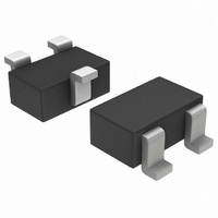
... I 200 Max 600 mA FSM I 300 mA FRM T −55 to 125 ° −55 to +150 °C stg BAT54SWT1G †For information on tape and reel specifications, 1 http://onsemi.com 30 VOLT DUAL SERIES SCHOTTKY BARRIER DIODES 1 2 ANODE CATHODE 3 CATHODE/ANODE MARKING DIAGRAM 3 SOT−323 B8M G CASE 419 G 1 STYLE 9 ...

Page 2

ELECTRICAL CHARACTERISTICS Characteristic Reverse Breakdown Voltage ( mA) R Total Capacitance ( 1.0 MHz) R Reverse Leakage ( Forward Voltage (I = 0.1 mAdc) F Forward Voltage (I = ...

Page 3

V , FORWARD VOLTAGE (VOLTS) F Figure 2. Forward Voltage 1000 T = 150°C A 100 10 1.0 0.1 0.01 0.001 ...

Page 4

... A1 *For additional information on our Pb−Free strategy and soldering details, please download the ON Semiconductor Soldering and Mounting Techniques Reference Manual, SOLDERRM/D. ON Semiconductor and are registered trademarks of Semiconductor Components Industries, LLC (SCILLC). SCILLC reserves the right to make changes without further notice to any products herein ...

Related keywords