BAT54SWT1G ON Semiconductor, BAT54SWT1G Datasheet - Page 2
BAT54SWT1G
Manufacturer Part Number
BAT54SWT1G
Description
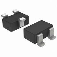
DIODE SCHOTTKY DUAL 30V SOT323
Manufacturer
ON Semiconductor
Specifications of BAT54SWT1G
Voltage - Forward (vf) (max) @ If
800mV @ 100mA
Current - Reverse Leakage @ Vr
2µA @ 25V
Current - Average Rectified (io) (per Diode)
200mA (DC)
Voltage - Dc Reverse (vr) (max)
30V
Reverse Recovery Time (trr)
5ns
Diode Type
Schottky
Speed
Small Signal =< 200mA (Io), Any Speed
Diode Configuration
1 Pair Series Connection
Mounting Type
Surface Mount
Package / Case
SC-70-3, SOT-323-3
Product
Schottky Diodes
Peak Reverse Voltage
30 V
Forward Continuous Current
0.2 A
Max Surge Current
0.6 A
Configuration
Dual Series
Recovery Time
5 ns
Forward Voltage Drop
0.8 V @ 0.1 A
Maximum Reverse Leakage Current
2 uA @ 25 V
Operating Temperature Range
- 55 C to + 125 C
Mounting Style
SMD/SMT
Current, Forward
200 mA
Package Type
SOT-323 (SC-70)
Power Dissipation
200 mW
Primary Type
Schottky Barrier
Speed, Switching
Fast
Temperature, Junction, Maximum
+125 °C
Temperature, Operating
-55 to +125 °C
Time, Recovery
5 ns
Voltage, Forward
0.52 V
Voltage, Reverse
30 V
Lead Free Status / RoHS Status
Lead free / RoHS Compliant
Other names
BAT54SWT1GOSTR
Available stocks
Company
Part Number
Manufacturer
Quantity
Price
Company:

Part Number:
BAT54SWT1G
Manufacturer:
ON Semiconductor
Quantity:
114 811
Company:
Part Number:
BAT54SWT1G
Manufacturer:
ON Semiconductor
Quantity:
16 650
Part Number:
BAT54SWT1G
Manufacturer:
ON/安森美
Quantity:
20 000


ELECTRICAL CHARACTERISTICS
+10 V
Reverse Breakdown Voltage
Total Capacitance
Reverse Leakage
Forward Voltage
Forward Voltage
Forward Voltage
Reverse Recovery Time
Forward Voltage
Forward Voltage
50 W OUTPUT
GENERATOR
(I
(V
(V
(I
(I
(I
(I
(I
(I
R
F
F
F
F
F
F
R
R
PULSE
= 0.1 mAdc)
= 30 mAdc)
= 100 mAdc)
= I
= 1.0 mAdc)
= 10 mAdc)
= 10 mA)
= 1.0 V, f = 1.0 MHz)
= 25 V)
820 W
R
= 10 mAdc, I
0.1 mF
100 mH
2 k
R(REC)
Characteristic
Notes: 1. A 2.0 kW variable resistor adjusted for a Forward Current (I
Notes:
Notes:
= 1.0 mAdc, Figure 1)
I
F
DUT
2. Input pulse is adjusted so I
3. t
Figure 1. Recovery Time Equivalent Test Circuit
p
» t
(T
A
rr
= 25°C unless otherwise noted) (EACH DIODE)
OSCILLOSCOPE
0.1 mF
50 W INPUT
SAMPLING
http://onsemi.com
R(peak)
2
V
R
is equal to 10 mA.
t
Symbol
r
V
INPUT SIGNAL
(BR)R
10%
90%
C
V
V
V
V
V
I
t
R
rr
T
F
F
F
F
F
t
p
T
Min
30
−
−
−
−
−
−
−
−
F
) of 10 mA.
I
I
R
F
0.22
0.41
0.52
0.29
0.35
Typ
7.6
0.5
−
−
(I
F
= I
at i
OUTPUT PULSE
R
= 10 mA; measured
R(REC)
Max
0.24
0.32
0.40
t
rr
2.0
0.5
0.8
5.0
10
−
i
R(REC)
= 1 mA)
= 1 mA
mAdc
Unit
Vdc
Vdc
Vdc
Vdc
Vdc
T
pF
ns
V
Related parts for BAT54SWT1G
Image
Part Number
Description
Manufacturer
Datasheet
Request
R

Part Number:
Description:
ON Semiconductor [VOLTAGE REGULATOR]
Manufacturer:
ON Semiconductor
Datasheet:
Part Number:
Description:
357-036-542-201 CARDEDGE 36POS DL .156 BLK LOPRO
Manufacturer:
ON Semiconductor
Datasheet:
Part Number:
Description:
357-036-542-201 CARDEDGE 36POS DL .156 BLK LOPRO
Manufacturer:
ON Semiconductor
Datasheet:
Part Number:
Description:
357-036-542-201 CARDEDGE 36POS DL .156 BLK LOPRO
Manufacturer:
ON Semiconductor
Datasheet:
Part Number:
Description:
357-036-542-201 CARDEDGE 36POS DL .156 BLK LOPRO
Manufacturer:
ON Semiconductor
Datasheet:
Part Number:
Description:
357-036-542-201 CARDEDGE 36POS DL .156 BLK LOPRO
Manufacturer:
ON Semiconductor
Datasheet:
Part Number:
Description:
357-036-542-201 CARDEDGE 36POS DL .156 BLK LOPRO
Manufacturer:
ON Semiconductor
Datasheet:
Part Number:
Description:
357-036-542-201 CARDEDGE 36POS DL .156 BLK LOPRO
Manufacturer:
ON Semiconductor
Datasheet:
Part Number:
Description:
357-036-542-201 CARDEDGE 36POS DL .156 BLK LOPRO
Manufacturer:
ON Semiconductor
Datasheet:
Part Number:
Description:
357-036-542-201 CARDEDGE 36POS DL .156 BLK LOPRO
Manufacturer:
ON Semiconductor
Datasheet:
Part Number:
Description:
357-036-542-201 CARDEDGE 36POS DL .156 BLK LOPRO
Manufacturer:
ON Semiconductor
Datasheet:
Part Number:
Description:
Manufacturer:
ON Semiconductor
Datasheet:
Part Number:
Description:
Manufacturer:
ON Semiconductor
Datasheet:
Part Number:
Description:
Manufacturer:
ON Semiconductor
Datasheet: