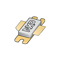
BLF6G20-110 NXP Semiconductors, BLF6G20-110 Datasheet - Page 4

BLF6G20-110
Manufacturer Part Number
BLF6G20-110
Description
RF MOSFET Small Signal LDMOS TNS
Manufacturer
NXP Semiconductors
Datasheet
1.BLF6G20-110.pdf
(10 pages)
Specifications of BLF6G20-110
Configuration
Single
Transistor Polarity
N-Channel
Resistance Drain-source Rds (on)
0.16 Ohms
Drain-source Breakdown Voltage
65 V
Gate-source Breakdown Voltage
13 V
Continuous Drain Current
29 A
Maximum Operating Temperature
+ 225 C
Mounting Style
SMD/SMT
Minimum Operating Temperature
- 65 C
Package / Case
SOT502B
Lead Free Status / RoHS Status
Lead free / RoHS Compliant
Other names
BLF6G20-110,112
Available stocks
Company
Part Number
Manufacturer
Quantity
Price
Company:
Part Number:
BLF6G20-110
Manufacturer:
NXP
Quantity:
1 000
Company:
Part Number:
BLF6G20-110
Manufacturer:
Humirel
Quantity:
5 000
Company:
Part Number:
BLF6G20-110,112
Manufacturer:
ZCOMM
Quantity:
1 400
NXP Semiconductors
BLF6G20-110_BLF6G20LS-110_3
Product data sheet
Fig 2.
(dB)
G
p
22
20
18
16
14
0
V
Two-tone CW power gain and drain efficiency
as function of peak envelope load power;
typical values
DS
= 30 V; I
20
7.2 One-tone CW
7.3 Two-tone CW
Dq
= 1400 mA; f = 1960 MHz.
40
Fig 1.
60
V
One-tone CW power gain and drain efficiency as function of load power;
typical values
DS
= 30 V; I
G
D
p
80
P
L(PEP)
001aaj073
Dq
(dB)
(W)
Rev. 03 — 13 January 2009
G
= 1400 mA; f = 1960 MHz.
100
BLF6G20-110; BLF6G20LS-110
p
22
20
18
16
14
60
45
30
15
0
(%)
0
D
20
Fig 3.
40
IMD3
(dBc)
10
30
50
70
60
0
V
Two-tone CW intermodulation distortion as a
function of peak envelope load power; typical
values
DS
80
= 30 V; I
G
20
D
p
100
Dq
= 1400 mA; f = 1960 MHz.
P
120
001aaj072
40
L(PEP)
140
(W)
Power LDMOS transistor
60
45
30
15
0
60
(%)
D
IMD3
IMD5
IMD7
© NXP B.V. 2009. All rights reserved.
80
P
L(PEP)
001aaj074
(W)
100
4 of 10


