BLF6G20-40,112 NXP Semiconductors, BLF6G20-40,112 Datasheet
BLF6G20-40,112
Specifications of BLF6G20-40,112


Related parts for BLF6G20-40,112


BLF6G20-40,112 Summary of contents
Page 1
... BLF6G20-40 Power LDMOS transistor Rev. 01 — 19 January 2009 1. Product profile 1.1 General description 40 W LDMOS power transistor for base station applications at frequencies from 1800 MHz to 2000 MHz. Table 1. RF performance at T Mode of operation 2-carrier W-CDMA [1] Test signal: 3GPP; test model 1; 64 DPCH; PAR = 7 0.01 % probability on CCDF per carrier; ...
Page 2
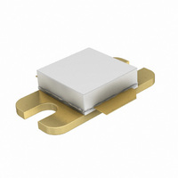
... Limiting values Parameter Conditions drain-source voltage gate-source voltage drain current storage temperature junction temperature Thermal characteristics Parameter thermal resistance from junction to case Rev. 01 — 19 January 2009 BLF6G20-40 Power LDMOS transistor Simplified outline Graphic symbol 1 [ Min - 0 ...
Page 3
... Mode of operation: 2-carrier W-CDMA; PAR 7 0.01 % probability on CCDF; 3GPP test model PDPCH performance at V class-AB production test circuit. Symbol ACPR 7.1 Ruggedness in class-AB operation The BLF6G20-40 is capable of withstanding a load mismatch corresponding to VSWR = through all phases under the following conditions 360 mA BLF6G20-40_1 Product data sheet Characteristics Conditions drain-source breakdown ...
Page 4
... Two-tone CW power gain and drain efficiency as functions of peak envelope load power; typical values BLF6G20-40_1 Product data sheet (dB 001aaj411 60 IMD D (%) (dBc ( 1843 MHz; 1 Fig 3. Rev. 01 — 19 January 2009 BLF6G20-40 Power LDMOS transistor 001aaj410 70 D (%) ( IMD3 20 30 IMD5 40 IMD7 360 mA 1843 MHz 1843.1 MHz. 2 Two-tone CW intermodulation distortion as a function of peak envelope load power ...
Page 5
... Test circuit for operation at 1805 MHz and 1880 MHz BLF6G20-40_1 Product data sheet 001aaj413 50 D ACPR (%) (dBc ( 1840.5 MHz; 1 Fig Rev. 01 — 19 January 2009 BLF6G20-40 Power LDMOS transistor 360 mA 1840.5 MHz 1845.5 MHz; carrier spacing 5 MHz. 2 2-carrier W-CDMA adjacent power channel ratio as function of average load power; typical values C8 C9 ...
Page 6
... Striplines are on a double copper-clad Rogers Duroid 5880 Printed-Circuit Board (PCB) ( See Table 8 for list of components. Fig 7. Component layout for 1805 MHz and 1880 MHz test circuit BLF6G20-40_1 Product data sheet C2 C1 Rev. 01 — 19 January 2009 BLF6G20-40 Power LDMOS transistor C14 C13 C8 C10 C9 C11 C12 C16 C7 C15 001aah551 = 2 ...
Page 7
... R1 Philips chip resistor [1] American technical ceramics type 100B or capacitor of same quality. [2] American technical ceramics type 100A or capacitor of same quality. BLF6G20-40_1 Product data sheet 7. Rev. 01 — 19 January 2009 BLF6G20-40 Power LDMOS transistor Value Remarks [1] 0.7 pF [1] 3 1.5 F [1] ...
Page 8
... REFERENCES JEDEC EIAJ Rev. 01 — 19 January 2009 BLF6G20-40 Power LDMOS transistor 1.70 20.45 9.91 15.24 0.25 0.51 1.35 20 ...
Page 9
... Power of the Dedicated Physical CHannel Radio Frequency Voltage Standing-Wave Ratio Wideband Code Division Multiple Access Release date Data sheet status 20090119 Product data sheet Rev. 01 — 19 January 2009 BLF6G20-40 Power LDMOS transistor Change notice Supersedes - - © NXP B.V. 2009. All rights reserved ...
Page 10
... Trademarks Notice: All referenced brands, product names, service names and trademarks are the property of their respective owners. http://www.nxp.com salesaddresses@nxp.com Rev. 01 — 19 January 2009 BLF6G20-40 Power LDMOS transistor © NXP B.V. 2009. All rights reserved ...
Page 11
... Please be aware that important notices concerning this document and the product(s) described herein, have been included in section ‘Legal information’. © NXP B.V. 2009. For more information, please visit: http://www.nxp.com For sales office addresses, please send an email to: salesaddresses@nxp.com All rights reserved. Date of release: 19 January 2009 Document identifier: BLF6G20-40_1 ...