BAV103,115 NXP Semiconductors, BAV103,115 Datasheet
BAV103,115
Specifications of BAV103,115
933699360115
BAV103 T/R
Available stocks


Related parts for BAV103,115


BAV103,115 Summary of contents
Page 1
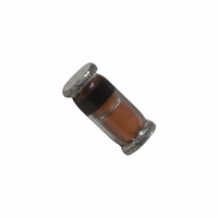
BAV102; BAV103 Single general-purpose switching diodes Rev. 4 — 6 August 2010 1. Product profile 1.1 General description Single general-purpose switching diodes, fabricated in planar technology, and encapsulated in small hermetically sealed glass SOD80C Surface-Mounted Device (SMD) packages. Table 1. ...
Page 2
... NXP Semiconductors 2. Pinning information Table 3. Pin 1 2 [1] The marking band indicates the cathode. 3. Ordering information Table 4. Type number BAV102 BAV103 4. Marking Table 5. Type number BAV102 BAV103 5. Limiting values Table 6. In accordance with the Absolute Maximum Rating System (IEC 60134). Symbol V RRM ...
Page 3
... NXP Semiconductors Table 6. In accordance with the Absolute Maximum Rating System (IEC 60134). Symbol P tot amb T stg [1] Pulse test: t [2] Device mounted on an FR4 PCB, single-sided copper, tin-plated and standard footprint °C prior to surge. [ Thermal characteristics Table 7. Symbol R th(j-a) R th(j-t) [1] Device mounted on an FR4 PCB, single-sided copper, tin-plated and standard footprint. ...
Page 4
... NXP Semiconductors 600 I F (mA) 400 (1) 200 150 °C; typical values (1) T amb = 25 °C; typical values (2) T amb = 25 °C; maximum values (3) T amb Fig 1. Forward current as a function of forward voltage (μ −1 10 − 100 Rmax Solid line: maximum values Dotted line: typical values Fig 3 ...
Page 5
... NXP Semiconductors 300 I F (mA) 200 100 0 0 100 FR4 PCB, standard footprint Fig 5. Forward current as a function of ambient temperature; derating curve 8. Test information D.U. Ω × ( Fig 7. Reverse recovery time test circuit and waveforms BAV102_BAV103 Product data sheet mbh278 300 V R (V) ...
Page 6
... NXP Semiconductors 9. Package outline Fig 8. 10. Packing information Table 9. The indicated -xxx are the last three digits of the 12NC ordering code. Type number BAV102 BAV103 [1] For further information and the availability of packing methods, see BAV102_BAV103 Product data sheet 0.3 3.7 3.3 ...
Page 7
... NXP Semiconductors 11. Soldering Fig 9. 2.90 Fig 10. Wave soldering footprint SOD80C BAV102_BAV103 Product data sheet 4.55 4.30 2.30 2.25 1.70 1.60 0.90 (2x) Reflow soldering footprint SOD80C 6.30 4.90 2.70 1.90 1.70 All information provided in this document is subject to legal disclaimers. Rev. 4 — 6 August 2010 BAV102 ...
Page 8
... NXP Semiconductors 12. Revision history Table 10. Revision history Document ID Release date BAV102_BAV103 v.4 20100806 • Modifications: Section 4 • Section 13 “Legal BAV102_BAV103_3 20070816 BAV100_2 19960917 BAV100_1 19960423 BAV102_BAV103 Product data sheet Single general-purpose switching diodes Data sheet status Product data sheet “Marking”: updated information” ...
Page 9
... In no event shall NXP Semiconductors be liable for any indirect, incidental, punitive, special or consequential damages (including - without limitation - lost profits, lost savings, business interruption, costs related to the removal or ...
Page 10
... NXP Semiconductors’ specifications such use shall be solely at customer’s own risk, and (c) customer fully indemnifies NXP Semiconductors for any liability, damages or failed product claims resulting from customer design and use of the product for automotive applications beyond NXP Semiconductors’ ...
Page 11
... NXP Semiconductors 15. Contents 1 Product profile . . . . . . . . . . . . . . . . . . . . . . . . . . 1 1.1 General description . . . . . . . . . . . . . . . . . . . . . 1 1.2 Features and benefits . . . . . . . . . . . . . . . . . . . . 1 1.3 Applications . . . . . . . . . . . . . . . . . . . . . . . . . . . 1 1.4 Quick reference data . . . . . . . . . . . . . . . . . . . . 1 2 Pinning information . . . . . . . . . . . . . . . . . . . . . . 2 3 Ordering information . . . . . . . . . . . . . . . . . . . . . 2 4 Marking . . . . . . . . . . . . . . . . . . . . . . . . . . . . . . . . 2 5 Limiting values Thermal characteristics . . . . . . . . . . . . . . . . . . 3 7 Characteristics . . . . . . . . . . . . . . . . . . . . . . . . . . 3 8 Test information . . . . . . . . . . . . . . . . . . . . . . . . . 5 9 Package outline . . . . . . . . . . . . . . . . . . . . . . . . . 6 10 Packing information . . . . . . . . . . . . . . . . . . . . . 6 11 Soldering ...