CMS02(TE12L) Toshiba, CMS02(TE12L) Datasheet
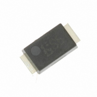
DIODE SCHOTTKY 30V 3A 3-4E1A

CMS02(TE12L)

Manufacturer Part Number
CMS02(TE12L)
Description
DIODE SCHOTTKY 30V 3A 3-4E1A
Manufacturer
Toshiba
Datasheet

Specifications of CMS02(TE12L)

Voltage - Forward (vf) (max) @ If
400mV @ 3A
Voltage - Dc Reverse (vr) (max)
30V
Current - Average Rectified (io)
3A
Current - Reverse Leakage @ Vr
500µA @ 30V
Diode Type
Schottky
Speed
Fast Recovery =< 500ns, > 200mA (Io)
Mounting Type
Surface Mount
Package / Case
3-4E1A (M-Flat)
Lead Free Status / RoHS Status
Contains lead / RoHS non-compliant
Reverse Recovery Time (trr)
-
Capacitance @ Vr, F
-
Other names
CMS02TR
Switching Mode Power Supply Applications
Portable Equipment Battery Applications
Absolute Maximum Ratings
Electrical Characteristics
Forward voltage: V
Average forward current: I
Repetitive peak reverse voltage: V
Suitable for compact assembly due to small surface-mount package
“M-FLAT
Repetitive peak reverse voltage
Average forward current
Peak one cycle surge forward current
(non-repetitive)
Junction temperature
Storage temperature
Note 1: Tℓ = 89.2°C: Rectangular waveform (α = 180°), V
Note 2: Using continuously under heavy loads (e.g. the application of
Peak forward voltage
Repetitive peak reverse current
Junction capacitance
Thermal resistance
high temperature/current/voltage and the significant change in temperature, etc.) may cause this product to
decrease in the reliability significantly even if the operating conditions (i.e. operating
temperature/current/voltage, etc.) are within the absolute maximum ratings.
Please design the appropriate reliability upon reviewing the Toshiba Semiconductor Reliability Handbook
(“Handling Precautions”/Derating Concept and Methods) and individual reliability data (i.e. reliability test
report and estimated failure rate, etc).
TM
Characteristics
Characteristics
” (Toshiba package name)
TOSHIBA Schottky Barrier Rectifier Trench Schottky Barrier Type
FM
= 0.40 V (max)
F (AV)
(Ta = 25°C)
= 3.0 A
RRM
(Ta = 25°C)
Symbol
I
V
F (AV)
I
T
FSM
RRM
T
Symbol
V
V
V
R
= 30 V
stg
R
I
I
j
FM (1)
FM (2)
FM (3)
th (j-a)
RRM
RRM
th (j-ℓ)
C
j
CMS02
40 (50 Hz)
I
I
I
V
V
V
Device mounted on a ceramic board
(soldering land: 2 mm × 2 mm)
Device mounted on a glass-epoxy
board
(soldering land: 6 mm × 6 mm)
FM
FM
FM
−40~125
−40~150
RRM
RRM
R
Rating
3.0
= 10 V, f = 1.0 MHz
30
= 0.5 A
= 1.0 A
= 3.0 A
1
(Note 1)
= 5 V
= 30 V
R
= 15 V
Test Condition
Unit
°C
°C
V
A
A
Weight: 0.023 g (typ.)
JEDEC
JEITA
TOSHIBA
Min
Typ.
0.27
0.30
0.37
0.05
0.07
170
3-4E1A
2006-11-13
0.40
Max
135
0.5
60
16
CMS02
Unit: mm
°C/W
Unit
mA
pF
V

Related parts for CMS02(TE12L)

CMS02(TE12L) Summary of contents

Page 1

... Please design the appropriate reliability upon reviewing the Toshiba Semiconductor Reliability Handbook (“Handling Precautions”/Derating Concept and Methods) and individual reliability data (i.e. reliability test report and estimated failure rate, etc) ...

Page 2

Marking Abbreviation Code Part No. S2 CMS02 Standard Soldering Pad 1.4 3.0 Handling Precaution Schottky barrier diodes have reverse current characteristics compared to other diodes. There is a possibility SBD may cause thermal runaway when it is used under high ...

Page 3

F F 100 125°C 75°C 1 25°C 0.1 0.0 0.2 0.4 0.6 0.8 1.0 Instantaneous forward voltage max – (AV) Device mounted on a ceramic board (board size: ...

Page 4

Surge forward current (non-repetitive 25° Number of cycles I – 100 Pulse test ...

Page 5

... Product shall not be used for or incorporated into any products or systems whose manufacture, use, or sale is prohibited under any applicable laws or regulations. • The information contained herein is presented only as guidance for Product use. No responsibility is assumed by TOSHIBA for any infringement of patents or any other intellectual property rights of third parties that may result from the use of Product. No license to any intellectual property right is granted by this document, whether express or implied, by estoppel or otherwise. • ...

Related keywords