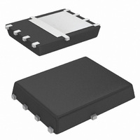
SI7983DP-T1-E3 Vishay, SI7983DP-T1-E3 Datasheet

SI7983DP-T1-E3
Specifications of SI7983DP-T1-E3
Available stocks
Related parts for SI7983DP-T1-E3
SI7983DP-T1-E3 Summary of contents
Page 1
... S1 6. Bottom View Ordering Information: Si7983DP-T1-E3 (Lead (Pb)-free) Si7983DP-T1-GE3 (Lead (Pb)-free and Halogen-free) ABSOLUTE MAXIMUM RATINGS T Parameter Drain-Source Voltage Gate-Source Voltage a Continuous Drain Current (T = 150 °C) J Pulsed Drain Current Continuous Source Current (Diode Conduction) a Maximum Power Dissipation Operating Junction and Storage Temperature Range ...
Page 2
... Si7983DP Vishay Siliconix SPECIFICATIONS °C, unless otherwise noted J Parameter Static Gate Threshold Voltage Gate-Body Leakage Zero Gate Voltage Drain Current a On-State Drain Current a Drain-Source On-State Resistance a Forward Transconductance a Diode Forward Voltage b Dynamic Total Gate Charge Gate-Source Charge Gate-Drain Charge Gate Resistance ...
Page 3
... S09-0272-Rev. B, 16-Feb-09 6000 5000 4000 3000 2000 1000 1.6 1.4 1.2 1.0 0.8 0 0.06 0.05 0.04 0.03 0. °C J 0.01 0.00 0.8 1.0 1.2 Si7983DP Vishay Siliconix C iss C oss C rss Drain-to-Source Voltage (V) DS Capacitance 100 - T Junction T emperature ( °C) J On-Resistance vs. Junction Temperature ...
Page 4
... Si7983DP Vishay Siliconix TYPICAL CHARACTERISTICS 25 °C, unless otherwise noted 0 600 µA D 0.3 0.2 0.1 0.0 - 0 Temperature (°C) J Threshold Voltage 2 1 Duty Cycle = 0.5 0.2 0.1 0.1 0.05 0.02 Single Pulse 0. www.vishay.com 4 75 100 125 150 100 Limited DS(on on) 1 Limited ° ...
Page 5
... Vishay Siliconix maintains worldwide manufacturing capability. Products may be manufactured at one of several qualified locations. Reliability data for Silicon Technology and Package Reliability represent a composite of all qualified locations. For related documents such as package/tape drawings, part marking, and reliability data, see www.vishay.com/ppg?72637. Document Number: 72637 S09-0272-Rev. B, 16-Feb- Square Wave Pulse Duration (s) Normalized Thermal Transient Impedance, Junction-to-Case Si7983DP Vishay Siliconix - www.vishay.com 5 ...
Page 6
... TYP. 3.98 TYP. 6.15 6.25 5.89 5.99 3.66 3.84 3.78 3.91 0.75 TYP. 1.27 BSC 1.27 TYP 0.61 0.71 0.61 0.71 0.13 0.20 - 12° 0.25 0.36 0.125 TYP. Package Information Vishay Siliconix Backside View of Single Pad Backside View of Dual Pad INCHES MIN ...
Page 7
... The minimum land pattern recommended to take full advantage of the PowerPAK thermal performance see Application Note 826, Recommended Minimum Pad Patterns With Outline Drawing Access for Vishay Sili- conix MOSFETs. Click on the PowerPAK SO-8 single in the index of this document. In this figure, the drain land pattern is given to make full contact to the drain pad on the PowerPAK package ...
Page 8
... Application Note 826, Recommended Minimum Pad Patterns With Outline Drawing Access for Vishay Siliconix MOSFETs. Click on the PowerPAK 1212-8 dual in the index of this doc- ument. The gap between the two drain pads is 24 mils. This matches the spacing of the two drain pads on the Pow- erPAK SO-8 dual package ...
Page 9
... No significant effect was observed Si7446DP 41 36 100 10000 0.00 Figure 6. Spreading Copper Junction-to-Ambient Performance AN821 Vishay Siliconix R vs. Spreading Copper 100 % Back Copper) 100 % 0.25 0.50 0.75 1.00 1.25 1.50 1.75 2 ...
Page 10
... AN821 Vishay Siliconix SYSTEM AND ELECTRICAL IMPACT OF PowerPAK SO-8 In any design, one must take into account the change in MOSFET r with temperature (Figure 7). DS(on) On-Resistance vs. Junction Temperature 1 1 1.4 1.2 1.0 0.8 0 Junction Temperature (°C) J Figure 7. MOSFET r vs. Temperature DS(on) A MOSFET generates internal heat due to the current passing through the channel ...
Page 11
... Application Note 826 Vishay Siliconix RECOMMENDED MINIMUM PADS FOR PowerPAK 0.024 (0.61) 0.026 (0.66) 0.050 (1.27) Return to Index Return to Index www.vishay.com 16 ® SO-8 Dual 0.260 (6.61) 0.150 (3.81) 0.024 (0.61) 0.032 (0.82) Recommended Minimum Pads Dimensions in Inches/(mm) 0.040 (1.02) Document Number: 72600 ...
Page 12
... Vishay product could result in personal injury or death. Customers using or selling Vishay products not expressly indicated for use in such applications their own risk and agree to fully indemnify and hold Vishay and its distributors harmless from and against any and all claims, liabilities, expenses and damages arising or resulting in connection with such use or sale, including attorneys fees, even if such claim alleges that Vishay or its distributor was negligent regarding the design or manufacture of the part ...


