BSO150N03 Infineon Technologies, BSO150N03 Datasheet - Page 3
BSO150N03
Manufacturer Part Number
BSO150N03
Description
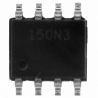
MOSFET N-CHAN 30V 7.6A DSO-8
Manufacturer
Infineon Technologies
Series
OptiMOS™r
Datasheet
1.BSO150N03.pdf
(9 pages)
Specifications of BSO150N03
Fet Type
2 N-Channel (Dual)
Fet Feature
Standard
Rds On (max) @ Id, Vgs
15 mOhm @ 9.1A, 10V
Drain To Source Voltage (vdss)
30V
Current - Continuous Drain (id) @ 25° C
7.6A
Vgs(th) (max) @ Id
2V @ 25µA
Gate Charge (qg) @ Vgs
15nC @ 5V
Input Capacitance (ciss) @ Vds
1890pF @ 15V
Power - Max
1.4W
Mounting Type
Surface Mount
Package / Case
DSO-8
Configuration
Dual Dual Drain
Transistor Polarity
N-Channel
Drain-source Breakdown Voltage
30 V
Gate-source Breakdown Voltage
+/- 20 V
Continuous Drain Current
7.6 A
Power Dissipation
1400 mW
Maximum Operating Temperature
+ 150 C
Mounting Style
SMD/SMT
Minimum Operating Temperature
- 55 C
Lead Free Status / RoHS Status
Lead free / RoHS Compliant
Other names
BSO150N03
BSO150N03INTR
BSO150N03XT
SP000077687
BSO150N03INTR
BSO150N03XT
SP000077687
Available stocks
Company
Part Number
Manufacturer
Quantity
Price
Company:

Part Number:
BSO150N03
Manufacturer:
Infineon Technologies
Quantity:
57 305
Company:
Part Number:
BSO150N03
Manufacturer:
LT
Quantity:
5 510
Part Number:
BSO150N03
Manufacturer:
INFINEON/英飞凌
Quantity:
20 000
Part Number:
BSO150N03M
Manufacturer:
INFINEON/英飞凌
Quantity:
20 000
Part Number:
BSO150N03MD
Manufacturer:
INFINEON/英飞凌
Quantity:
20 000
Part Number:
BSO150N03MD G
Manufacturer:
INFINEON/英飞凌
Quantity:
20 000
Company:
Part Number:
BSO150N03MDG
Manufacturer:
INFINEON
Quantity:
10 000


Rev. 1.6
4)
Parameter
Dynamic characteristics
Input capacitance
Output capacitance
Reverse transfer capacitance
Turn-on delay time
Rise time
Turn-off delay time
Fall time
Gate Charge Characteristics
Gate to source charge
Gate charge at threshold
Gate to drain charge
Switching charge
Gate charge total
Gate plateau voltage
Gate charge total, sync. FET
Output charge
Reverse Diode
Diode continous forward current
Diode pulse current
Diode forward voltage
Reverse recovery charge
See figure 16 for gate charge parameter definition
4)
Symbol Conditions
C
C
C
t
t
t
t
Q
Q
Q
Q
Q
V
Q
Q
I
I
V
Q
d(on)
r
d(off)
f
S
S,pulse
plateau
SD
iss
oss
rss
gs
g(th)
gd
sw
g
g(sync)
oss
rr
V
f =1 MHz
V
I
V
V
V
V
V
T
V
T
V
di
D
page 3
A
j
GS
DD
DD
GS
DS
GS
DD
GS
R
=4.5 A, R
=25 °C
F
=25 °C
=12 V, I
/dt =400 A/µs
=0.1 V,
=0 V, V
=15 V, V
=15 V, I
=0 to 5 V
=0 to 5 V
=15 V, V
=0 V, I
F
F
DS
=2 A,
G
=I
D
GS
=2.7 Ω
GS
=4.5 A,
=15 V,
S
=10 V,
=0 V
,
min.
-
-
-
-
-
-
-
-
-
-
-
-
-
-
-
-
-
-
-
Values
1420
0.75
typ.
510
5.3
4.0
3.0
3.9
2.3
2.6
4.3
2.8
9.6
67
21
11
12
-
-
-
max.
BSO150N03
1890
680
100
7.9
6.0
4.5
5.2
3.0
4.0
6.1
31
15
13
16
36
10
2
1
-
Unit
pF
ns
nC
V
nC
A
V
nC
2008-01-16
Related parts for BSO150N03
Image
Part Number
Description
Manufacturer
Datasheet
Request
R

Part Number:
Description:
Manufacturer:
Infineon Technologies AG
Datasheet:
Part Number:
Description:
Manufacturer:
Infineon Technologies AG
Datasheet:
Part Number:
Description:
Manufacturer:
Infineon Technologies AG
Datasheet:
Part Number:
Description:
Manufacturer:
Infineon Technologies AG
Datasheet:
Part Number:
Description:
Manufacturer:
Infineon Technologies AG
Datasheet:
Part Number:
Description:
Manufacturer:
Infineon Technologies AG
Datasheet:
Part Number:
Description:
Manufacturer:
Infineon Technologies AG
Datasheet:
Part Number:
Description:
16-bit microcontroller with 2x2 KByte RAM
Manufacturer:
Infineon Technologies AG
Datasheet:
Part Number:
Description:
NPN silicon RF transistor
Manufacturer:
Infineon Technologies AG
Datasheet:
Part Number:
Description:
NPN silicon RF transistor
Manufacturer:
Infineon Technologies AG
Datasheet:
Part Number:
Description:
NPN silicon RF transistor
Manufacturer:
Infineon Technologies AG
Datasheet:
Part Number:
Description:
NPN silicon RF transistor
Manufacturer:
Infineon Technologies AG
Datasheet:
Part Number:
Description:
Si-MMIC-amplifier in SIEGET 25-technologie
Manufacturer:
Infineon Technologies AG
Datasheet:
Part Number:
Description:
IGBT Power Module
Manufacturer:
Infineon Technologies AG
Datasheet:
Part Number:
Description:
IC for switching-mode power supplies
Manufacturer:
Infineon Technologies AG
Datasheet: