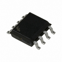
FDS8958B Fairchild Semiconductor, FDS8958B Datasheet - Page 8

FDS8958B
Manufacturer Part Number
FDS8958B
Description
MOSFET N/P-CH 30V TRENCH 8-SOIC
Manufacturer
Fairchild Semiconductor
Series
PowerTrench®r
Datasheet
1.FDS8958B.pdf
(10 pages)
Specifications of FDS8958B
Fet Type
N and P-Channel
Fet Feature
Logic Level Gate
Rds On (max) @ Id, Vgs
26 mOhm @ 6.4A, 10V
Drain To Source Voltage (vdss)
30V
Current - Continuous Drain (id) @ 25° C
6.4A, 4.5A
Vgs(th) (max) @ Id
3V @ 250µA
Gate Charge (qg) @ Vgs
12nC @ 10V
Input Capacitance (ciss) @ Vds
540pF @ 15V
Power - Max
900mW
Mounting Type
Surface Mount
Package / Case
8-SOIC (3.9mm Width)
Configuration
Dual Dual Drain
Transistor Polarity
N and P-Channel
Resistance Drain-source Rds (on)
0.026 Ohm @ 10 V @ N Channel
Drain-source Breakdown Voltage
30 V
Gate-source Breakdown Voltage
+/- 20 V @ N Channel or +/- 25 V @ P Channel
Continuous Drain Current
6.4 A @ N Channel or 4.5 A @ P Channel
Power Dissipation
1600 mW
Maximum Operating Temperature
+ 150 C
Mounting Style
SMD/SMT
Minimum Operating Temperature
- 55 C
Lead Free Status / RoHS Status
Lead free / RoHS Compliant
Other names
FDS8958BTR
Available stocks
Company
Part Number
Manufacturer
Quantity
Price
Company:
Part Number:
FDS8958B
Manufacturer:
FSC
Quantity:
5 000
Company:
Part Number:
FDS8958B
Manufacturer:
JKY
Quantity:
2 200
Part Number:
FDS8958B
Manufacturer:
FAIRCHILD/ن»™ç«¥
Quantity:
20 000
Company:
Part Number:
FDS8958B-NL
Manufacturer:
FAIRCHILD
Quantity:
12 637
Part Number:
FDS8958B-NL
Manufacturer:
FAIRCHILD/ن»™ç«¥
Quantity:
20 000
FDS8958B Rev.B
©2008 Fairchild Semiconductor Corporation
Typical Characteristics (Q2 P-Channel)
0.01
100
10
0.1
10
8
6
4
2
0
1
8
7
6
5
4
3
2
1
0.01
0.01
0
Figure 21. Gate Charge Characteristics
I
THIS AREA IS
LIMITED BY r
D
= -4.5 A
Figure 23. Unclamped Inductive
Figure 25. Forward Bias Safe
-V
3
DS
0.1
t
Switching Capability
SINGLE PULSE
T
R
T
AV
, DRAIN to SOURCE VOLTAGE (V)
J
A
θ
DS(on)
, TIME IN AVALANCHE (ms)
JA
= MAX RATED
= 25
Operating Area
Q
0.1
= 135
g
V
T
, GATE CHARGE (nC)
J
DD
o
C
6
= 125
= -10 V
o
C/W
1
o
C
V
T
J
DD
= 25
9
= -20 V
o
1
C
V
DD
10
= -15 V
12
100 ms
1 ms
10 ms
1 s
10 s
0.1 ms
DC
100
10
15
8
T
J
= 25 °C unless otherwise noted
200
100
10
10
10
10
10
10
10
10
2000
1000
0.5
10
100
1
-2
-3
-4
-5
-6
-7
-8
-9
10
30
Figure 26. Single Pulse Maximum Power
0
0.1
-4
V
f = 1 MHz
V
GS
GS
Figure 22. Capacitance vs Drain
10
= 0V
5
= 0 V
-3
-V
-V
DS
GS ,
Figure 24. Ig vs Vgs
10
V
t, PULSE WIDTH (sec)
, DRAIN TO SOURCE VOLTAGE (V)
10
to Source Voltage
T
GS
GATE TO SOURCE VOLTAGE(V)
J
-2
= 125
= -10 V
Dissipation
10
15
1
o
C
-1
T
J
= 25
20
1
o
C
SINGLE PULSE
R
T
25
10
A
θ
JA
= 25
= 135
www.fairchildsemi.com
10
o
C
100
30
C
C
C
o
oss
rss
iss
C/W
1000
35
30


