SI7945DP-T1-E3 Vishay, SI7945DP-T1-E3 Datasheet - Page 8
SI7945DP-T1-E3
Manufacturer Part Number
SI7945DP-T1-E3
Description
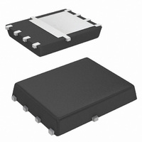
MOSFET DUAL P-CH 30V 8-SOIC
Manufacturer
Vishay
Series
TrenchFET®r
Specifications of SI7945DP-T1-E3
Transistor Polarity
Dual P-Channel
Fet Type
2 P-Channel (Dual)
Fet Feature
Logic Level Gate
Rds On (max) @ Id, Vgs
20 mOhm @ 10.9A, 10V
Drain To Source Voltage (vdss)
30V
Current - Continuous Drain (id) @ 25° C
7A
Vgs(th) (max) @ Id
3V @ 250µA
Gate Charge (qg) @ Vgs
74nC @ 10V
Power - Max
1.4W
Mounting Type
Surface Mount
Package / Case
PowerPAK® SO-8 Dual
Minimum Operating Temperature
- 55 C
Configuration
Dual Dual Drain
Drain-source Breakdown Voltage
30 V
Gate-source Breakdown Voltage
+/- 20 V
Continuous Drain Current
7 A
Power Dissipation
1400 mW
Maximum Operating Temperature
+ 150 C
Mounting Style
SMD/SMT
Continuous Drain Current Id
-10.9A
Drain Source Voltage Vds
-30V
On Resistance Rds(on)
31mohm
Rds(on) Test Voltage Vgs
20V
Threshold Voltage Vgs Typ
-3V
Lead Free Status / RoHS Status
Lead free / RoHS Compliant
Lead Free Status / RoHS Status
Lead free / RoHS Compliant, Lead free / RoHS Compliant
Other names
SI7945DP-T1-E3TR
Available stocks
Company
Part Number
Manufacturer
Quantity
Price

Part Number:
SI7945DP-T1-E3
Manufacturer:
VISHAY/威世
Quantity:
20 000


AN821
Vishay Siliconix
PowerPAK SO-8 DUAL
The pin arrangement (drain, source, gate pins) and the
pin dimensions of the PowerPAK SO-8 dual are the
same as standard SO-8 dual devices. Therefore, the
PowerPAK device connection pads match directly to
those of the SO-8. As in the single-channel package,
the only exception is the extended drain connection
area. Manufacturers can likewise take immediate
advantage of the PowerPAK SO-8 dual devices by
mounting them to existing SO-8 dual land patterns.
To take the advantage of the dual PowerPAK SO-8’s
thermal performance, the minimum recommended
land pattern can be found in Application Note 826,
Recommended Minimum Pad Patterns With Outline
Drawing Access for Vishay Siliconix MOSFETs. Click
on the PowerPAK 1212-8 dual in the index of this doc-
ument.
The gap between the two drain pads is 24 mils. This
matches the spacing of the two drain pads on the Pow-
erPAK SO-8 dual package.
REFLOW SOLDERING
Vishay Siliconix surface-mount packages meet solder
reflow reliability requirements. Devices are subjected
to solder reflow as a test preconditioning and are then
reliability-tested using temperature cycle, bias humid-
ity, HAST, or pressure pot. The solder reflow tempera-
ture profile used, and the temperatures and time
duration, are shown in Figures 3 and 4.
www.vishay.com
2
3 °C(max)
140 - 170 °C
Figure 3. Solder Reflow Temperatures and Time Durations
Maximum peak temperature at 240 °C is allowed.
Pre-Heating Zone
60 s (min)
210 - 220 °C
3 °C(max)
For the lead (Pb)-free solder profile, see http://
www.vishay.com/doc?73257.
Ramp-Up Rate
Time at Maximum Temperature
Temperature at 155 ± 15 °C
Temperature Above 180 °C
Maximum Temperature
Ramp-Down Rate
Figure 3. Solder Reflow Temperature Profile
Reflow Zone
50 s (max)
10 s (max)
183 °C
4 ° C/s (max)
+ 6 °C /Second Maximum
120 Seconds Maximum
70 - 180 Seconds
240 + 5/- 0 °C
20 - 40 Seconds
+ 6 °C/Second Maximum
Document Number 71622
28-Feb-06
Related parts for SI7945DP-T1-E3
Image
Part Number
Description
Manufacturer
Datasheet
Request
R

Part Number:
Description:
Dual P-channel 30-v D-s Mosfet
Manufacturer:
Vishay
Datasheet:

Part Number:
Description:
MOSFET DL P-CH 30V PPAK 8-SOIC
Manufacturer:
Vishay
Datasheet:
Part Number:
Description:
357-036-542-201 CARDEDGE 36POS DL .156 BLK LOPRO
Manufacturer:
Vishay
Datasheet:
Part Number:
Description:
357-036-542-201 CARDEDGE 36POS DL .156 BLK LOPRO
Manufacturer:
Vishay
Datasheet:
Part Number:
Description:
357-036-542-201 CARDEDGE 36POS DL .156 BLK LOPRO
Manufacturer:
Vishay
Datasheet:
Part Number:
Description:
357-036-542-201 CARDEDGE 36POS DL .156 BLK LOPRO
Manufacturer:
Vishay
Datasheet:
Part Number:
Description:
357-036-542-201 CARDEDGE 36POS DL .156 BLK LOPRO
Manufacturer:
Vishay
Datasheet:
Part Number:
Description:
357-036-542-201 CARDEDGE 36POS DL .156 BLK LOPRO
Manufacturer:
Vishay
Datasheet:
Part Number:
Description:
357-036-542-201 CARDEDGE 36POS DL .156 BLK LOPRO
Manufacturer:
Vishay
Datasheet:
Part Number:
Description:
357-036-542-201 CARDEDGE 36POS DL .156 BLK LOPRO
Manufacturer:
Vishay
Datasheet:
Part Number:
Description:
357-036-542-201 CARDEDGE 36POS DL .156 BLK LOPRO
Manufacturer:
Vishay
Datasheet:
Part Number:
Description:
357-036-542-201 CARDEDGE 36POS DL .156 BLK LOPRO
Manufacturer:
Vishay
Datasheet:
Part Number:
Description:
357-036-542-201 CARDEDGE 36POS DL .156 BLK LOPRO
Manufacturer:
Vishay
Datasheet:
Part Number:
Description:
357-036-542-201 CARDEDGE 36POS DL .156 BLK LOPRO
Manufacturer:
Vishay
Datasheet:
Part Number:
Description:
357-036-542-201 CARDEDGE 36POS DL .156 BLK LOPRO
Manufacturer:
Vishay
Datasheet: