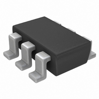
FDC3601N Fairchild Semiconductor, FDC3601N Datasheet - Page 3

FDC3601N
Manufacturer Part Number
FDC3601N
Description
MOSFET N-CH DUAL 100V SSOT-6
Manufacturer
Fairchild Semiconductor
Series
PowerTrench®r
Datasheet
1.FDC3601N.pdf
(5 pages)
Specifications of FDC3601N
Fet Type
2 N-Channel (Dual)
Fet Feature
Logic Level Gate
Rds On (max) @ Id, Vgs
500 mOhm @ 1A, 10V
Drain To Source Voltage (vdss)
100V
Current - Continuous Drain (id) @ 25° C
1A
Vgs(th) (max) @ Id
4V @ 250µA
Gate Charge (qg) @ Vgs
5nC @ 10V
Input Capacitance (ciss) @ Vds
153pF @ 50V
Power - Max
700W
Mounting Type
Surface Mount
Package / Case
6-SSOT, SuperSOT-6
Configuration
Dual
Transistor Polarity
N-Channel
Resistance Drain-source Rds (on)
0.5 Ohm @ 10 V
Forward Transconductance Gfs (max / Min)
3.6 S
Drain-source Breakdown Voltage
100 V
Gate-source Breakdown Voltage
+/- 20 V
Continuous Drain Current
1 A
Power Dissipation
960 mW
Maximum Operating Temperature
+ 150 C
Mounting Style
SMD/SMT
Minimum Operating Temperature
- 55 C
Module Configuration
Dual
Continuous Drain Current Id
1A
Drain Source Voltage Vds
100V
On Resistance Rds(on)
500mohm
Rds(on) Test Voltage Vgs
10V
Rohs Compliant
Yes
Threshold Voltage Vgs Typ
2.6V
Lead Free Status / RoHS Status
Lead free / RoHS Compliant
Available stocks
Company
Part Number
Manufacturer
Quantity
Price
Company:
Part Number:
FDC3601N
Manufacturer:
FSC
Quantity:
15 600
Company:
Part Number:
FDC3601N
Manufacturer:
Fairchild Semiconductor
Quantity:
59 148
Typical Characteristics
4.5
1.5
4
3
2
1
0
6
3
0
0
1.5
Figure 3. On-Resistance Variation with
2.6
2.2
1.8
1.4
0.6
0.2
V
Figure 1. On-Region Characteristics.
1
GS
-50
Figure 5. Transfer Characteristics.
6.0V
V
= 10V
DS
V
I
= 5V
D
GS
= 1.0A
-25
=10V
V
2
2.5
V
GS
4.5V
DS
T
, GATE TO SOURCE VOLTAGE (V)
, DRAIN-SOURCE VOLTAGE (V)
0
J
, JUNCTION TEMPERATURE (
Temperature.
5.0V
25
T
A
3.5
= 125
4
50
o
C
-55
o
75
C
4.0V
25
o
C
4.5
100
o
6
C)
125
5.5
150
8
Figure 6. Body Diode Forward Voltage Variation
1.25
0.75
0.25
0.0001
0.5
0.001
1.6
1.4
1.2
0.8
1
0.01
Figure 2. On-Resistance Variation with
Figure 4. On-Resistance Variation with
0.1
with Source Current and Temperature.
1
2
10
1
0
0
Drain Current and Gate Voltage.
V
GS
= 0V
Gate-to-Source Voltage.
V
0.2
GS
V
SD
V
= 4.0V
4
GS
, BODY DIODE FORWARD VOLTAGE (V)
1
, GATE TO SOURCE VOLTAGE (V)
I
0.4
D
T
, DRAIN CURRENT (A)
A
= 125
4.5V
o
C
6
5.0V
2
0.6
T
T
25
6.0V
A
A
o
= 125
= 25
C
0.8
10V
o
C
o
C
-55
3
8
o
C
FDC3601N Rev C(W)
I
D
1
= 0.5A
1.2
4
10


