FDS6900AS Fairchild Semiconductor, FDS6900AS Datasheet
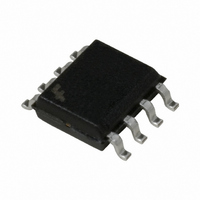
MOSFET N-CH DUAL 30V 8SOIC

FDS6900AS

Manufacturer Part Number
FDS6900AS
Description
MOSFET N-CH DUAL 30V 8SOIC
Manufacturer
Fairchild Semiconductor
Series
PowerTrench®r
Datasheet

Specifications of FDS6900AS

Fet Type
2 N-Channel (Dual)
Fet Feature
Logic Level Gate
Rds On (max) @ Id, Vgs
27 mOhm @ 6.9A, 10V
Drain To Source Voltage (vdss)
30V
Current - Continuous Drain (id) @ 25° C
6.9A, 8.2A
Vgs(th) (max) @ Id
3V @ 250µA
Gate Charge (qg) @ Vgs
15nC @ 10V
Input Capacitance (ciss) @ Vds
600pF @ 15V
Power - Max
900mW
Mounting Type
Surface Mount
Package / Case
8-SOIC (3.9mm Width)
Configuration
Dual
Transistor Polarity
N-Channel
Resistance Drain-source Rds (on)
0.022 Ohms
Forward Transconductance Gfs (max / Min)
25 S, 21 S
Drain-source Breakdown Voltage
30 V
Gate-source Breakdown Voltage
+/- 20 V
Continuous Drain Current
6.9 A, 8.2 A
Power Dissipation
2 W
Maximum Operating Temperature
+ 150 C
Mounting Style
SMD/SMT
Minimum Operating Temperature
- 55 C
Lead Free Status / RoHS Status
Lead free / RoHS Compliant

Available stocks

Company
Part Number
Manufacturer
Quantity
Price
Part Number:
FDS6900AS
Manufacturer:
Fairchild Semiconductor
Quantity:
1 787
Part Number:
FDS6900AS
Manufacturer:
MAXIM
Quantity:
136
Part Number:
FDS6900AS
Manufacturer:
FAIRCHILD
Quantity:
8 000
Part Number:
FDS6900AS
Manufacturer:
FAIRCHILD/仙童
Quantity:
20 000
Company:
Part Number:
FDS6900AS
Quantity:
1 540
Part Number:
FDS6900AS-NL
Manufacturer:
FAIRCHILD
Quantity:
50 000
Part Number:
FDS6900AS_NL
Manufacturer:
WOOYUNG
Quantity:
10 523
FDS6900AS
Dual N-Ch PowerTrench
General Description
The FDS6900AS is designed to replace two single SO-
8 MOSFETs and Schottky diode in synchronous DC:DC
power supplies that provide various peripheral voltages
for notebook computers and other battery powered
electronic devices. FDS6900AS contains two unique
30V, N-channel, logic level, PowerTrench MOSFETs
designed to maximize power conversion efficiency.
The high-side switch (Q1) is designed with specific
emphasis on reducing switching losses while the low-
side switch (Q2) is optimized to reduce conduction
losses. Q2 also includes an integrated Schottky diode
using Fairchild’s monolithic SyncFET technology.
©2005 Fairchild Semiconductor Corporation
Absolute Maximum Ratings
V
V
I
P
T
Thermal Characteristics
R
R
Package Marking and Ordering Information
Symbol
D
J
DSS
GSS
D
θJA
θJC
, T
Device Marking
FDS6900AS
FDS6900AS
STG
SO-8
Drain-Source Voltage
Gate-Source Voltage
Drain Current
Power Dissipation for Dual Operation
Power Dissipation for Single Operation
Operating and Storage Junction Temperature Range
Thermal Resistance, Junction-to-Ambient
Thermal Resistance, Junction-to-Case
Pin 1
D
G1
S1D2
D
FDS6900AS_NL
S1D2
SO-
D
- Continuous
- Pulsed
FDS6900AS
S1D2
D
Device
Parameter
®
D1
S
SyncFET
D1
S
(Note 4)
G2
S
S2
T
G
A
= 25°C unless otherwise noted
Reel Size
13”
13”
(Note 1a)
(Note 1a)
(Note 1b)
(Note 1c)
(Note 1a)
(Note 1)
Features
Q2:
Q1:
6.9A, 30V
100% R
8.2A, 30V
Optimized to minimize conduction losses
Includes SyncFET Schottky body diode
Optimized for low switching losses
Low Gate Charge (11nC typical)
G
Q2
±20
8.2
30
30
(Gate Resistance) Tested
1
2
4
3
Tape width
R
R
R
R
–55 to +150
12mm
12mm
DS(on)
DS(on)
DS(on)
DS(on)
Q1
Q2
Dual N-Channel SyncFet
1.6
0.9
78
40
2
1
= 22mΩ @ V
= 28mΩ @ V
= 27mΩ @ V
= 34mΩ @ V
Q1
±20
6.9
30
20
5
8
7
6
GS
GS
GS
GS
May 2005
FDS6900AS Rev B(X)
= 10V
= 4.5V
= 10V
= 4.5V
2500 units
2500 units
Quantity
Units
°C/W
°C/W
°C
W
V
V
A

Related parts for FDS6900AS

FDS6900AS Summary of contents

Page 1

... FDS6900AS Dual N-Ch PowerTrench General Description The FDS6900AS is designed to replace two single SO- 8 MOSFETs and Schottky diode in synchronous DC:DC power supplies that provide various peripheral voltages for notebook computers and other battery powered electronic devices. FDS6900AS contains two unique 30V, N-channel, logic level, PowerTrench MOSFETs designed to maximize power conversion efficiency ...

Page 2

... Referenced to 25° 8 8 125° 125° 1.0 MHz Ω 10V GEN Ω 4 GEN mV/° µA Q2 500 Q1 1 ±100 1 1.9 3 mV/°C Q2 –3.2 Q1 –4 mΩ 570 pF Q1 600 Q2 180 pF Q1 150 Ω Q2 2.8 4.9 Q1 2.2 3 FDS6900AS Rev B (X) ...

Page 3

... Scale letter size paper 2. Pulse Test: Pulse Width < 300µs, Duty Cycle < 2.0% 3. See “SyncFET Schottky body diode characteristics” below. 4. FDS6900AS_NL is a lead free product. The FDS6900AS_NL marking will appear on the reel label. (continued 25°C unless otherwise noted A ...

Page 4

... C 0.01 0.001 0 3.5 4 Figure 6. Body Diode Forward Voltage Variation with Source Current and Temperature. 4.0V 4.5V 5.0V 6.0V 10V DRAIN CURRENT ( 125 GATE TO SOURCE VOLTAGE (V) GS Gate-to-Source Voltage -55 C 0.2 0.4 0.6 0 BODY DIODE FORWARD VOLTAGE (V) SD FDS6900AS Rev B ( ...

Page 5

... Figure 10. Single Pulse Maximum 0.01 0 TIME (sec 1MHz iss C oss DRAIN TO SOURCE VOLTAGE (V) DS SINGLE PULSE R = 135°C/W θ 25° 100 t , TIME (sec) 1 Power Dissipation. R ( θJA θ 135 °C/W θJA P(pk (t) θ Duty Cycle 100 FDS6900AS Rev B (X) 30 1000 1000 ...

Page 6

... Figure 17. Body Diode Forward Voltage Variation with Source Current and Temperature. 4.0V 4.5V 5.0V 6. DRAIN CURRENT ( 3. 125 GATE TO SOURCE VOLTAGE (V) GS Gate-to-Source Voltage 125 -55 C 0.2 0.4 0.6 0 BODY DIODE FORWARD VOLTAGE (V) SD FDS6900AS Rev B (X) 10V 20 10 1.2 ...

Page 7

... Figure 21. Single Pulse Maximum 0.01 0 TIME (sec MHz iss C oss DRAIN TO SOURCE VOLTAGE (V) DS SINGLE PULSE R = 135°C/W θ 25° 100 1000 t , TIME (sec) 1 Power Dissipation. R ( θJA θ 135 C/W θJA P(pk (t) θ Duty Cycle 100 1000 FDS6900AS Rev B (X) 30 ...

Page 8

... Schottky diode in parallel with a MOSFET. Figure 23 shows the reverse recovery characteristic of the FDS6900AS. Time: 10nS/DIV Figure 23. FDS6900AS SyncFET body diode reverse recovery characteristic. For comparison purposes, Figure 24 shows the reverse recovery characteristics of the body diode of an equivalent size MOSFET produced without SyncFET (FDS6690) ...

Page 9

... Pulse Width ≤ 1µs Duty Cycle ≤ 0.1% Figure 30. Switching Time Test Circuit + Figure 27. Unclamped Inductive Waveforms + 10V DUT Charge, (nC) Figure 29. Gate Charge Waveform d(ON 90 DUT 50% 10% 0V Figure 31. Switching Time Waveforms BV DSS G(TOT OFF t d(OFF 90% 10% 10% 90% 50% Pulse Width FDS6900AS Rev B (X) ...

Page 10

... TRADEMARKS The following are registered and unregistered trademarks Fairchild Semiconductor owns or is authorized to use and is not intended exhaustive list of all such trademarks. FAST ® ACEx™ ActiveArray™ FASTr™ Bottomless™ FPS™ Build it Now™ FRFET™ CoolFET™ ...

Related keywords