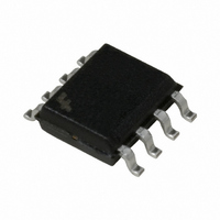
FDS6900AS Fairchild Semiconductor, FDS6900AS Datasheet - Page 9

FDS6900AS
Manufacturer Part Number
FDS6900AS
Description
MOSFET N-CH DUAL 30V 8SOIC
Manufacturer
Fairchild Semiconductor
Series
PowerTrench®r
Datasheet
1.FDS6900AS.pdf
(10 pages)
Specifications of FDS6900AS
Fet Type
2 N-Channel (Dual)
Fet Feature
Logic Level Gate
Rds On (max) @ Id, Vgs
27 mOhm @ 6.9A, 10V
Drain To Source Voltage (vdss)
30V
Current - Continuous Drain (id) @ 25° C
6.9A, 8.2A
Vgs(th) (max) @ Id
3V @ 250µA
Gate Charge (qg) @ Vgs
15nC @ 10V
Input Capacitance (ciss) @ Vds
600pF @ 15V
Power - Max
900mW
Mounting Type
Surface Mount
Package / Case
8-SOIC (3.9mm Width)
Configuration
Dual
Transistor Polarity
N-Channel
Resistance Drain-source Rds (on)
0.022 Ohms
Forward Transconductance Gfs (max / Min)
25 S, 21 S
Drain-source Breakdown Voltage
30 V
Gate-source Breakdown Voltage
+/- 20 V
Continuous Drain Current
6.9 A, 8.2 A
Power Dissipation
2 W
Maximum Operating Temperature
+ 150 C
Mounting Style
SMD/SMT
Minimum Operating Temperature
- 55 C
Lead Free Status / RoHS Status
Lead free / RoHS Compliant
Available stocks
Company
Part Number
Manufacturer
Quantity
Price
Company:
Part Number:
FDS6900AS
Manufacturer:
Fairchild Semiconductor
Quantity:
1 787
Company:
Part Number:
FDS6900AS
Manufacturer:
MAXIM
Quantity:
136
Part Number:
FDS6900AS
Manufacturer:
FAIRCHILD/ن»™ç«¥
Quantity:
20 000
Company:
Part Number:
FDS6900AS-NL
Manufacturer:
FAIRCHILD
Quantity:
50 000
Company:
Part Number:
FDS6900AS_NL
Manufacturer:
WOOYUNG
Quantity:
10 523
Typical Characteristics
Figure 26. Unclamped Inductive Load Test
Figure 28. Gate Charge Test Circuit
Figure 30. Switching Time Test
+
R
-
10V
V
GE
vary t
required peak I
V
V
GS
Drain Current
I
Circuit
R
GS
GS
g(REF
10µF
Same type as
P
V
GEN
0V
Duty Cycle ≤ 0.1%
Pulse Width ≤ 1µs
to obtain
DS
V
tp
V
GS
50kΩ
GS
V
Circuit
AS
DS
1µF
I
AS
0.01Ω
DUT
L
DUT
R
DUT
L
+
-
+
-
+
-
V
V
V
DD
DD
DD
Figure 27. Unclamped Inductive
10V
V
V
V
Figure 29. Gate Charge Waveform
GS
DS
GS
Figure 31. Switching Time Waveforms
0V
0V
10%
Q
t
d(ON)
90%
GS
Waveforms
Charge, (nC)
t
50%
ON
Q
10%
Pulse Width
I
G(TOT)
t
AS
Q
r
GD
t
P
BV
t
AV
DSS
t
)
d(OFF
90%
50%
t
OFF
V
t
10%
f
FDS6900AS Rev B (X)
DS
V
90%
DD


