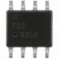
FDS9958 Fairchild Semiconductor, FDS9958 Datasheet - Page 2

FDS9958
Manufacturer Part Number
FDS9958
Description
MOSFET P-CH 60V DUAL SO-8
Manufacturer
Fairchild Semiconductor
Series
PowerTrench®r
Datasheet
1.FDS9958.pdf
(6 pages)
Specifications of FDS9958
Fet Type
2 P-Channel (Dual)
Fet Feature
Logic Level Gate
Rds On (max) @ Id, Vgs
105 mOhm @ 2.9A, 10V
Drain To Source Voltage (vdss)
60V
Current - Continuous Drain (id) @ 25° C
2.9A
Vgs(th) (max) @ Id
3V @ 250µA
Gate Charge (qg) @ Vgs
23nC @ 10V
Input Capacitance (ciss) @ Vds
1020pF @ 30V
Power - Max
900mW
Mounting Type
Surface Mount
Package / Case
8-SOIC (3.9mm Width)
Configuration
Dual Dual Drain
Transistor Polarity
P-Channel
Resistance Drain-source Rds (on)
0.105 Ohm @ 10 V
Drain-source Breakdown Voltage
60 V
Gate-source Breakdown Voltage
+/- 20 V
Continuous Drain Current
2.9 A
Power Dissipation
2000 mW
Maximum Operating Temperature
+ 150 C
Mounting Style
SMD/SMT
Minimum Operating Temperature
- 55 C
Lead Free Status / RoHS Status
Lead free / RoHS Compliant
Other names
FDS9958TR
Available stocks
Company
Part Number
Manufacturer
Quantity
Price
Company:
Part Number:
FDS9958
Manufacturer:
FSC
Quantity:
15 000
Company:
Part Number:
FDS9958
Manufacturer:
Fairchild Semiconductor
Quantity:
33 440
Part Number:
FDS9958
Manufacturer:
ON/ه®‰و£®ç¾ژ
Quantity:
20 000
Company:
Part Number:
FDS9958-NL
Manufacturer:
FAIRCHILD
Quantity:
12 652
Part Number:
FDS9958-NL
Manufacturer:
FAIRCHILD/ن»™ç«¥
Quantity:
20 000
©2007 Fairchild Semiconductor Corporation
FDS9958 Rev.C
Electrical Characteristics
Off Characteristics
On Characteristics
Dynamic Characteristics
Switching Characteristics
Drain-Source Diode Characteristics
NOTES:
1. R
2. Pulse Test: Pulse Width < 300µs, Duty cycle < 2.0%.
3. UIL condition: Starting T
BV
∆BV
I
I
V
r
g
C
C
C
t
t
t
t
Q
Q
Q
Q
V
t
Q
∆V
DSS
GSS
∆T
d(on)
r
d(off)
f
rr
DS(on)
FS
the user's board design.
GS(th)
SD
iss
oss
rss
∆T
g
g
gs
gd
rr
Symbol
θJA
DSS
J
GS(th)
DSS
J
is determined with the device mounted on a 1in
Drain to Source Breakdown Voltage
Breakdown Voltage Temperature
Coefficient
Zero Gate Voltage Drain Current
Gate to Source Leakage Current
Gate to Source Threshold Voltage
Gate to Source Threshold Voltage
Temperature Coefficient
Static Drain to Source On Resistance
Forward Transconductance
Input Capacitance
Output Capacitance
Reverse Transfer Capacitance
Turn-On Delay Time
Rise Time
Turn-Off Delay Time
Fall Time
Total Gate Charge
Total Gate Charge
Gate to Source Charge
Gate to Drain “Miller” Charge
Source to Drain Diode Forward Voltage
Reverse Recovery Time
Reverse Recovery Charge
J
= 25°C, L = 3mH, I
Parameter
AS
= 6A, V
2
T
pad 2 oz copper pad on a 1.5 x 1.5 in. board of FR-4 material. R
a) 78°C/W when
J
DD
= 25°C unless otherwise noted
mounted on a 1 in
pad of 2 oz copper
= 60V, V
GS
= 10V.
2
V
V
V
V
V
I
V
V
V
V
V
f = 1MHz
I
I
V
V
V
V
I
D
D
D
F
GS
GS
GS
GS
DD
DD
GS
GS
GS
DS
GS
GS
DS
GS
= -250µA, referenced to 25°C
= -2.9A, di/dt = 100A/µs
= -250µA, V
= -250µA, referenced to 25°C
= 0V to -10V
= 0V to -4.5V
= -10V, I
= -30V, V
= -30V, I
= -10V, R
= -48V,
= 0V
= V
= -10V, I
= -4.5V, I
= -5V, I
= 0V, I
= ±20V, V
2
DS
Test Conditions
, I
S
D
D
= -1.3A
D
D
D
GS
GEN
= -2.9A
GS
DS
= -2.9A,
D
= -250µA
= -2.9A, T
= -2.9A
= -2.5A
= 0V,
= 0V
= 0V
= 6Ω
V
I
T
D
DD
J
= -2.9A
= 125°C
(Note 2)
= -30V,
J
= 125°C
θJC
b) 135°C/W when
is guaranteed by design while R
mounted on a
minimun pad
Min
-1.0
-60
Typ
-1.6
-0.8
103
131
765
-52
7.7
26
21
82
90
40
27
16
4
6
3
6
8
2
3
±100
1020
Max
-100
-1.2
-3.0
105
135
190
120
θCA
65
12
10
43
12
23
12
42
35
-1
www.fairchildsemi.com
is determined by
mV/°C
mV/°C
Units
mΩ
µA
nA
nC
pF
pF
pF
nC
nC
nC
nC
ns
ns
ns
ns
ns
V
V
S
V


