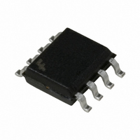
FDS6912 Fairchild Semiconductor, FDS6912 Datasheet - Page 4

FDS6912
Manufacturer Part Number
FDS6912
Description
MOSFET N-CH DUAL PWM OPT 8-SOIC
Manufacturer
Fairchild Semiconductor
Series
PowerTrench®r
Specifications of FDS6912
Fet Type
2 N-Channel (Dual)
Fet Feature
Logic Level Gate
Rds On (max) @ Id, Vgs
28 mOhm @ 6A, 10V
Drain To Source Voltage (vdss)
30V
Current - Continuous Drain (id) @ 25° C
6A
Vgs(th) (max) @ Id
3V @ 250µA
Gate Charge (qg) @ Vgs
10nC @ 5V
Input Capacitance (ciss) @ Vds
740pF @ 15V
Power - Max
900mW
Mounting Type
Surface Mount
Package / Case
8-SOIC (3.9mm Width)
Module Configuration
Dual
Transistor Polarity
N Channel
Continuous Drain Current Id
6A
Drain Source Voltage Vds
30V
On Resistance Rds(on)
28mohm
Rds(on) Test Voltage Vgs
10V
Rohs Compliant
Yes
Dc
0452
Lead Free Status / RoHS Status
Lead free / RoHS Compliant
Available stocks
Company
Part Number
Manufacturer
Quantity
Price
Company:
Part Number:
FDS6912
Manufacturer:
FSC
Quantity:
5 550
Part Number:
FDS6912
Manufacturer:
FAIRCHILD/ن»™ç«¥
Quantity:
20 000
Company:
Part Number:
FDS6912-NL
Manufacturer:
FSC
Quantity:
68 500
Company:
Part Number:
FDS6912-NL
Manufacturer:
SIEMENS
Quantity:
5 000
Part Number:
FDS6912-NL
Manufacturer:
FAIRCHILD/ن»™ç«¥
Quantity:
20 000
Company:
Part Number:
FDS6912A
Manufacturer:
FAIRCHIL
Quantity:
29 332
Company:
Part Number:
FDS6912A
Manufacturer:
FSC
Quantity:
50 000
Part Number:
FDS6912A
Manufacturer:
FAIRCHILD/ن»™ç«¥
Quantity:
20 000
Typical Characteristics
10
0.01
100
8
6
4
2
0
0.1
Figure 9. Maximum Safe Operating Area.
10
1
0
Figure 7. Gate Charge Characteristics.
0.1
0.001
0.01
I
D
R
0.1
= 6A
DS(ON)
0.0001
SINGLE PULSE
1
R
JA
V
T
GS
A
LIMIT
= 135
2
= 25
= 10V
o
o
C
C/W
D = 0.5
V
DS
, DRAIN-SOURCE VOLTAGE (V)
0.2
Q
4
0.1
1
g
0.05
, GATE CHARGE (nC)
0.02
0.001
DC
0.01
10s
Transient thermal response will change depending on the circuit board design.
Thermal characterization performed using the conditions described in Note 1c.
SINGLE PULSE
V
DS
6
1s
Figure 11. Transient Thermal Response Curve.
= 10V
100ms
15V
10ms
10
8
0.01
1ms
20V
100 s
10
100
12
0.1
t
1
, TIME (sec)
800
600
400
200
50
40
30
20
10
0
0.001
0
Figure 8. Capacitance Characteristics.
0
Figure 10. Single Pulse Maximum
C
1
rss
0.01
V
Power Dissipation.
DS
5
, DRAIN TO SOURCE VOLTAGE (V)
0.1
C
10
oss
t
1
, TIME (sec)
1
10
P(pk)
Duty Cycle, D = t
T
R
J
R
10
- T
100
JA
JA
C
(t) = r(t) * R
A
iss
t
SINGLE PULSE
= 135°C/W
1
R
= P * R
t
15
2
JA
T
A
= 135°C/W
FDS6912A Rev D(W)
100
= 25°C
V
f = 1MHz
GS
JA
1
JA
(t)
= 0 V
/ t
2
1000
1000
20


