IRF7309PBF International Rectifier, IRF7309PBF Datasheet
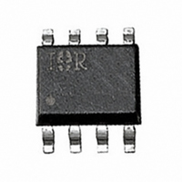
MOSFET N+P 30V 3A 8-SOIC

IRF7309PBF

Manufacturer Part Number
IRF7309PBF
Description
MOSFET N+P 30V 3A 8-SOIC
Manufacturer
International Rectifier
Series
HEXFET®r
Type
Power MOSFETr
Datasheets

Specifications of IRF7309PBF

Fet Type
N and P-Channel
Fet Feature
Standard
Rds On (max) @ Id, Vgs
50 mOhm @ 2.4A, 10V
Drain To Source Voltage (vdss)
30V
Current - Continuous Drain (id) @ 25° C
4A, 3A
Vgs(th) (max) @ Id
1V @ 250µA
Gate Charge (qg) @ Vgs
25nC @ 4.5V
Input Capacitance (ciss) @ Vds
520pF @ 15V
Power - Max
1.4W
Mounting Type
Surface Mount
Package / Case
8-SOIC (3.9mm Width)
Number Of Elements
2
Polarity
N/P
Channel Mode
Enhancement
Drain-source On-volt
30V
Gate-source Voltage (max)
±20V
Power Dissipation
1.4W
Operating Temp Range
-55C to 150C
Operating Temperature Classification
Military
Mounting
Surface Mount
Pin Count
8
Package Type
SOIC
Lead Free Status / RoHS Status
Lead free / RoHS Compliant
HEXFET
Description
Thermal Resistance
Absolute Maximum Ratings
Fifth Generation HEXFETs from International Rectifier utilize advanced processing
techniques to achieve the lowest possible on-resistance per silicon area. This
benefit, combined with the fast switching speed and ruggedized device design for
which HEXFET Power MOSFETs are well known, provides the designer with an
extremely efficient device for use in a wide variety of applications.
The SO-8 has been modified through a customized leadframe for enhanced
thermal characteristics and multiple-die capability making it ideal in a variety of
power applications. With these improvements, multiple devices can be used in an
application with dramatically reduced board space. The package is designed for
vapor phase, infra-red, or wave soldering techniques. Power dissipation of greater
than 0.8W is possible in a typical PCB mount application.
** When mounted on 1" square PCB (FR-4 or G-10 Material).
I
I
I
I
P
V
dv/dt
T
R
D
D
D
DM
J,
D
GS
@ T
@ T
@ T
JA
Generation V Technology
Ultra Low On-Resistance
Dual N and P Channel Mosfet
Surface Mount
Available in Tape & Reel
Dynamic dv/dt Rating
Fast Switching
@T
T
STG
For recommended footprint and soldering techniques refer to application note #AN-994.
A
A
A
A
= 25°C
= 25°C
= 70°C
= 25°C
®
Power MOSFET
Parameter
10 Sec. Pulse Drain Current, V
Continuous Drain Current, V
Pulsed Drain Current
Power Dissipation (PCB Mount)**
Linear Derating Factor (PCB Mount)**
Gate-to-Source Voltage
Peak Diode Recovery dv/dt
Junction and Storage Temperature Range
Junction-to-Amb. (PCB Mount, steady state)**
Parameter
PRELIMINARY
GS
GS
GS
@ 10V
@ 10V
@ 10V
G2
G1
S2
S1
147
N-CHANNEL MOSFET
1
2
3
4
P-CHANNEL MOSFET
Top View
Min.
––––
N-Channel
4.7
4.0
3.2
6.9
16
8
7
6
5
D1
D1
D2
D2
-55 to + 150
Max.
0.011
± 20
1.4
Typ.
––––
R
V
DS(on)
IRF7309
DSS
P-Channel
-3.5
-3.0
-2.4
-6.0
-12
PD - 9.1243B
SO-8
0.050
N-Ch
Max.
30V
90
Units
0.10
W/°C
P-Ch
V/ns
-30V
°C
Units
W
°C/W
A
A
A
A
V

Related parts for IRF7309PBF

IRF7309PBF Summary of contents

Page 1

... Dynamic dv/dt Rating Fast Switching Description Fifth Generation HEXFETs from International Rectifier utilize advanced processing techniques to achieve the lowest possible on-resistance per silicon area. This benefit, combined with the fast switching speed and ruggedized device design for which HEXFET Power MOSFETs are well known, provides the designer with an extremely efficient device for use in a wide variety of applications ...

Page 2

IRF7309 Electrical Characteristics @ T Parameter V Drain-to-Source Breakdown Voltage (BR)DSS Breakdown Voltage Temp. Coefficient (BR)DSS J R Static Drain-to-Source On-Resistance DS(ON) V Gate Threshold Voltage GS(th) g Forward Transconductance fs I Drain-to-Source Leakage Current DSS I ...

Page 3

VGS TOP 15V 10V 8.0V 7.0V 6.0V 5.5V 5.0V BOTTOM 4.5V 100 4.5V 10 20µs PULSE WIDTH T = 25° 0 Drain-to-Source Voltage (V) DS Fig 1. Typical Output Characteristics ...

Page 4

IRF7309 1000 1MHz iss rss oss ds gd 800 C iss 600 C oss 400 200 ...

Page 5

T , Ambient Temperature (°C) A Fig 9. Max. Drain Current Vs. Ambient Temp. Fig 11a. Gate Charge Test Circuit 100 VGS TOP - 15V - 10V - 8.0V - 7.0V ...

Page 6

IRF7309 100 T = 25° 150° 20µs PULSE WIDTH Gate-to-Source Voltage (V) GS Fig 14. Typical Transfer Characteristics 1000 1MHz GS C ...

Page 7

T = 150° 25° 0.1 0.0 0.3 0.6 0 Source-to-Drain Voltage (V) SD Fig 18. Typical Source-Drain Diode Forward Voltage 3.0 2.0 1.0 0 100 T , AmbientTemperature ...

Page 8

IRF7309 Fig 22b. Gate Charge Test Circuit 100 D = 0.50 0.20 10 0.10 0.05 0.02 0.01 1 SINGLE PULSE (THERMAL RESPONSE) 0.1 0.00001 0.0001 0.001 Fig 23. Maximum Effective Transient Thermal Impedance, Junction-to-Ambient Refer to the Appendix Section for ...

Related keywords