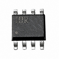
IRF7379 International Rectifier, IRF7379 Datasheet

IRF7379
Specifications of IRF7379
Available stocks
Related parts for IRF7379
IRF7379 Summary of contents
Page 1
... Peak Diode Recovery dv/ Junction and Storage Temperature Range J, STG Thermal Resistance Ratings Parameter R Maximum Junction-to-Ambient JA www.irf.com FET FET Parameter N-Channel @ 10V GS @ 10V 91625 IRF7379 ® HEXFET Power MOSFET N-Ch P- 30V -30V DSS 0.045 0.090 DS(on Max. P-Channel 30 -30 5.8 -4.3 4.6 -3 ...
Page 2
... IRF7379 Electrical Characteristics @ T Parameter V Drain-to-Source Breakdown Voltage (BR)DSS Breakdown Voltage Temp. Coefficient (BR)DSS J R Static Drain-to-Source On-Resistance DS(ON) V Gate Threshold Voltage GS(th) g Forward Transconductance fs I Drain-to-Source Leakage Current DSS I Gate-to-Source Forward Leakage GSS Q Total Gate Charge g Q Gate-to-Source Charge gs Q Gate-to-Drain ("Miller") Charge ...
Page 3
... - rce V olta Fig 3. Typical Transfer Characteristics www.irf.com N-Channel 1000 100 4.5V 20µ 25° ° µ IRF7379 VGS TOP 15V 10V 8.0V 7.0V 6.0V 5.5V 5.0V BOTTOM 4. µ 150° 0 in-to-S ource V olta Fig 2. Typical Output Characteristics 150 ° ° 0.1 ...
Page 4
... IRF7379 2 4.0A D 1.5 1.0 0.5 0.0 -60 -40 - Junction Tem perature (° Fig 5. Normalized On-Resistance Vs. Temperature 4 N-Channel 0.20 0.16 0.12 0.08 0. 10V 0. Fig 6. Typical On-Resistance Vs. Drain 0.08 0.07 0.06 0. 5.8A 0.04 0. Gate-to-Source Voltage (V) GS Fig 7. Typical On-Resistance Vs. Gate Voltage VGS = 4.5V VGS = 10V ...
Page 5
... SINGLE PULSE (THERMAL RESPONSE) 0.1 0.00001 0.0001 Fig 10. Maximum Effective Transient Thermal Impedance, Junction-to-Ambient www.irf.com N-Channel 100 0.001 0. Rectangular Pulse Duration (sec) 1 IRF7379 2. 24V FIG Total G ate C harge ( Fig 9. Typical Gate Charge Vs. Gate-to-Source Voltage P DM Notes: 1. Duty factor ...
Page 6
... IRF7379 VGS TOP - 15V - 10V - 8.0V - 7.0V - 6.0V - 5.5V - 5.0V BOTTOM - 4. 0 rain-to-S ourc e V oltage ( Fig 11. Typical Output Characteristics 100 ° - lta Fig 13. Typical Transfer Characteristics 6 P-Channel - µ 5° 100 ° µ 100 VGS TOP - 15V - 10V - 8.0V - 7. ...
Page 7
... Fig 15. Normalized On-Resistance Vs. Temperature 0.16 0.14 0.12 0.10 0.08 0.06 www.irf.com P-Channel 0.50 0.40 0.30 0. 100 120 140 160 Fig 16. Typical On-Resistance Vs. Drain ID = -4. Gate-to-Source Voltage (V) GS Fig 17. Typical On-Resistance Vs. Gate Voltage IRF7379 VGS = -4.5V VGS = -10V Drain Current (A) D Current ...
Page 8
... IRF7379 iss iss C oss rss - rce V oltage ( Fig 18. Typical Capacitance Vs. Drain-to-Source Voltage 100 D = 0.50 0.20 10 0.10 0.05 0.02 1 0.01 SINGLE PULSE (THERMAL RESPONSE) 0.1 0.00001 0.0001 Fig 20. Maximum Effective Transient Thermal Impedance, Junction-to-Ambient 8 P-Channel 0.001 0. Rectangular Pulse Duration (sec -3. -24V FIG ...
Page 9
... MOLD PROTRUSIONS NOT TO EXCEED 0.25 (.006). DIMENSIONS IS THE LENGTH OF LEAD FOR SOLDERING TO A SUBSTRATE.. 6 Part Marking Information SO8 www.irf.com 45° 0.10 (.004 IRF7379 INCHES DIM MIN MAX A .0532 .0688 A1 .0040 .0098 B .014 .018 C .0075 .0098 D .189 .196 E .150 .157 e .050 BASIC e1 ...
Page 10
... IRF7379 Tape & Reel Information SO8 Dimensions are shown in millimeters (inches) 8.1 ( .318 ) 7.9 ( .312 ) ( & - SIO ILLIM LIN EIA-48 1 & E IA-541. WORLD HEADQUARTERS: 233 Kansas St., El Segundo, California 90245, Tel: (310) 322 3331 IR GREAT BRITAIN: Hurst Green, Oxted, Surrey RH8 9BB, UK Tel 1883 732020 IR FAR EAST: K& ...


