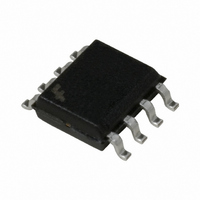
FDS9431A Fairchild Semiconductor, FDS9431A Datasheet - Page 4

FDS9431A
Manufacturer Part Number
FDS9431A
Description
MOSFET P-CH 20V 3.5A 8SOIC
Manufacturer
Fairchild Semiconductor
Type
Power MOSFETr
Datasheet
1.FDS9431A.pdf
(5 pages)
Specifications of FDS9431A
Fet Type
MOSFET P-Channel, Metal Oxide
Fet Feature
Logic Level Gate
Rds On (max) @ Id, Vgs
130 mOhm @ 3.5A, 4.5V
Drain To Source Voltage (vdss)
20V
Current - Continuous Drain (id) @ 25° C
3.5A
Vgs(th) (max) @ Id
1V @ 250µA
Gate Charge (qg) @ Vgs
8.5nC @ 4.5V
Input Capacitance (ciss) @ Vds
405pF @ 10V
Power - Max
1W
Mounting Type
Surface Mount
Package / Case
8-SOIC (3.9mm Width)
Configuration
Single Quad Drain Triple Source
Transistor Polarity
P-Channel
Resistance Drain-source Rds (on)
0.13 Ohm @ 4.5 V
Forward Transconductance Gfs (max / Min)
6.5 S
Drain-source Breakdown Voltage
20 V
Gate-source Breakdown Voltage
+/- 8 V
Continuous Drain Current
3.5 A
Power Dissipation
2500 mW
Maximum Operating Temperature
+ 150 C
Mounting Style
SMD/SMT
Minimum Operating Temperature
- 55 C
Number Of Elements
1
Polarity
P
Channel Mode
Enhancement
Drain-source On-res
0.13Ohm
Drain-source On-volt
20V
Gate-source Voltage (max)
±8V
Output Power (max)
Not RequiredW
Frequency (max)
Not RequiredMHz
Noise Figure
Not RequireddB
Power Gain
Not RequireddB
Drain Efficiency
Not Required%
Operating Temp Range
-55C to 150C
Operating Temperature Classification
Military
Mounting
Surface Mount
Pin Count
8
Package Type
SOIC N
Lead Free Status / RoHS Status
Lead free / RoHS Compliant
Other names
FDS9431A
Available stocks
Company
Part Number
Manufacturer
Quantity
Price
Company:
Part Number:
FDS9431A
Manufacturer:
Fairchild Semiconductor
Quantity:
49 116
Company:
Part Number:
FDS9431A
Manufacturer:
FSC
Quantity:
2 440
Part Number:
FDS9431A
Manufacturer:
FAIRCHILD/ن»™ç«¥
Quantity:
20 000
Company:
Part Number:
FDS9431A-NL
Manufacturer:
FAIRCHILD
Quantity:
12 644
Part Number:
FDS9431A-NL
Manufacturer:
FAIRCHILD/ن»™ç«¥
Quantity:
20 000
Typical Characteristics
0. 05
0. 01
5
4
3
2
1
0
0 .5
Figure 9. Maximum Safe Operating Area.
Figure 7. Gate Charge Characteristics.
50
10
0
3
0 .1
I
D
SINGLE PULSE
R
= -1.6A
SING L E PUL SE
R
V
JA
T
V
GS
J A
T = 2 5°C
A
G S
= 125°C/W
A
0. 0 05
0. 0 02
0. 0 01
= 135 °C/W
A
= 25°C
= -4.5V
0 .05
0 .02
0 .01
= -4.5V
0 .3
0.5
0.2
0.1
0.0 001
1
- V
2
D S
D = 0 .5
, DR A IN -SO UR C E V OLTA GE (V)
Q g , G ATE C H ARG E (nC )
0 .2
1
0 .1
0 . 0 5
0 . 0 2
4
0. 0 01
Figure 11. Transient Thermal Response Curve.
2
V
0 .0 1
D S
= -5V
S i n g l e P u l s e
-15V
Thermal characterization performed using the conditions described in Note 1c.
Transient themal response will change depending on the circuit board design.
5
(continued)
6
10
0 .01
30
8
t , TI ME (s e c )
0.1
1
2000
1000
500
200
100
50
40
30
20
10
Figure 8. Capacitance Characteristics.
50
0
0.001
0.1
Figure 10. Single Pulse Maximum
f = 1 M Hz
V
1
G S
0.2
= 0 V
0.01
-V
Power Dissipation.
DS
, D R A IN T O S OU R CE V OLTA GE (V)
0.5
SINGLE PULSE TIME (SEC)
0.1
P(p k )
10
D u t y C y c l e, D = t /t
1
T - T = P * R
R
J
R
J A
t
1
A
(t) = r(t) * R
J A
1
2
t
2
= 125°C / W
SINGLE PULSE
R
JA
T
JA
= 125
A
100
= 25
10
5
( t )
J A
1
o
o
2
C/W
C
10
300
C iss
C rss
C oss
FDS9431A Rev. A2
100
20
1000


