SI3433BDV-T1-E3 Vishay, SI3433BDV-T1-E3 Datasheet - Page 2
SI3433BDV-T1-E3
Manufacturer Part Number
SI3433BDV-T1-E3
Description
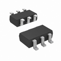
MOSFET P-CH 20V 4.3A 6-TSOP
Manufacturer
Vishay
Series
TrenchFET®r
Specifications of SI3433BDV-T1-E3
Transistor Polarity
P-Channel
Fet Type
MOSFET P-Channel, Metal Oxide
Fet Feature
Logic Level Gate
Rds On (max) @ Id, Vgs
42 mOhm @ 5.6A, 4.5V
Drain To Source Voltage (vdss)
20V
Current - Continuous Drain (id) @ 25° C
4.3A
Vgs(th) (max) @ Id
850mV @ 250µA
Gate Charge (qg) @ Vgs
18nC @ 10V
Power - Max
1.1W
Mounting Type
Surface Mount
Package / Case
6-TSOP
Minimum Operating Temperature
- 55 C
Configuration
Single Quad Drain
Resistance Drain-source Rds (on)
0.042 Ohm @ 4.5 V
Drain-source Breakdown Voltage
20 V
Gate-source Breakdown Voltage
+/- 8 V
Continuous Drain Current
4.3 A
Power Dissipation
1100 mW
Maximum Operating Temperature
+ 150 C
Mounting Style
SMD/SMT
Continuous Drain Current Id
-5.6A
Drain Source Voltage Vds
-20V
On Resistance Rds(on)
42mohm
Rds(on) Test Voltage Vgs
-4.5V
Threshold Voltage Vgs Typ
-450mV
Lead Free Status / RoHS Status
Lead free / RoHS Compliant
Lead Free Status / RoHS Status
Lead free / RoHS Compliant, Lead free / RoHS Compliant
Other names
SI3433BDV-T1-E3TR
Available stocks
Company
Part Number
Manufacturer
Quantity
Price

Part Number:
SI3433BDV-T1-E3
Manufacturer:
VISHAY/威世
Quantity:
20 000


Notes
a.
b.
www.vishay.com
2-2
Si3433
Vishay Siliconix
SPECIFICATIONS (T
Static
Gate Threshold Voltage
Gate-Body Leakage
Zero Gate Voltage Drain Current
Zero Gate Voltage Drain Current
On-State Drain Current
Drain-Source On-State Resistance
Forward Transconductance
Diode Forward Voltage
Dynamic
Total Gate Charge
Gate-Source Charge
Gate-Drain Charge
Turn-On Delay Time
Rise Time
Turn-Off Delay Time
Fall Time
Source-Drain Reverse Recovery Time
TYPICAL CHARACTERISTICS (25_C UNLESS NOTED)
Pulse test; pulse width v 300 ms, duty cycle v 2%.
Guaranteed by design, not subject to production testing.
20
16
12
8
4
0
0.0
b
Parameter
0.5
V
a
a
DS
1.0
Output Characteristics
a
- Drain-to-Source Voltage (V)
1.5
a
J
= 25_C UNLESS OTHERWISE NOTED)
2.0
V
GS
2.5
= 5 thru 2.5 V
Symbol
3.0
V
r
I
DS(on)
DS(on)
t
I
t
I
I
GS(th)
D(on)
V
Q
Q
d(off)
d(on)
GSS
DSS
DSS
g
Q
t
SD
t
t
rr
fs
gs
gd
r
f
g
3.5
1.5 V
2 V
1 V
4.0
New Product
V
DS
I
V
D
DS
^ - 1 A, V
= - 10 V, V
I
F
V
= - 16 V, V
V
V
V
V
V
V
V
V
GS
= - 1.7 A, di/dt = 100 A/ms
DS
GS
I
DS
V
S
DS
DS
DD
DD
Test Condition
GS
DS
= - 1.7 A, V
= - 4.5 V, I
= - 5 V, V
= V
= - 2.5 V, I
= - 16 V, V
= - 5 V, I
= - 10 V, R
= - 10 V, R
= - 1.8 V, I
= 0 V, V
GEN
GS
GS
GS
, I
= - 4.5 V, I
= - 4.5 V, R
D
= 0 V, T
GS
D
GS
= - 250 mA
D
D
GS
GS
D
= - 5.6 A
L
L
= - 4.5 V
= - 4.8 A
= - 5.6 A
= 10 W
= 10 W
= - 1 A
= "8 V
= 0 V
= 0 V
J
20
16
12
D
= 85_C
G
8
4
0
= - 5.6 A
0.0
= 6 W
0.5
V
GS
Transfer Characteristics
Min
- 0.45
- 20
- Gate-to-Source Voltage (V)
1.0
T
C
1.5
0.025
0.048
0.066
Typ
11.5
- 0.7
1.7
25_C
16
18
25
80
45
30
= - 55_C
3
S-00624—Rev. A, 03-Apr-00
Document Number: 71160
2.0
"100
Max
0.042
0.057
0.080
- 1.2
160
125_C
17
36
50
90
50
- 1
- 5
2.5
Unit
nA
mA
mA
nC
ns
V
A
W
S
V
3.0
Related parts for SI3433BDV-T1-E3
Image
Part Number
Description
Manufacturer
Datasheet
Request
R

Part Number:
Description:
P CHANNEL MOSFET, -20V, 4.3A, TSOP
Manufacturer:
Vishay
Datasheet:

Part Number:
Description:
P-channel 1.8-v G-s Mosfet
Manufacturer:
Vishay
Datasheet:

Part Number:
Description:
MOSFET 20V 5.6A 1.1W
Manufacturer:
Vishay/Siliconix
Datasheet:
Part Number:
Description:
P-channel 1.8-v G-s Mosfet
Manufacturer:
Vishay
Datasheet:
Part Number:
Description:
357-036-542-201 CARDEDGE 36POS DL .156 BLK LOPRO
Manufacturer:
Vishay
Datasheet:
Part Number:
Description:
357-036-542-201 CARDEDGE 36POS DL .156 BLK LOPRO
Manufacturer:
Vishay
Datasheet:
Part Number:
Description:
357-036-542-201 CARDEDGE 36POS DL .156 BLK LOPRO
Manufacturer:
Vishay
Datasheet:
Part Number:
Description:
357-036-542-201 CARDEDGE 36POS DL .156 BLK LOPRO
Manufacturer:
Vishay
Datasheet:
Part Number:
Description:
357-036-542-201 CARDEDGE 36POS DL .156 BLK LOPRO
Manufacturer:
Vishay
Datasheet:
Part Number:
Description:
357-036-542-201 CARDEDGE 36POS DL .156 BLK LOPRO
Manufacturer:
Vishay
Datasheet:
Part Number:
Description:
357-036-542-201 CARDEDGE 36POS DL .156 BLK LOPRO
Manufacturer:
Vishay
Datasheet:
Part Number:
Description:
357-036-542-201 CARDEDGE 36POS DL .156 BLK LOPRO
Manufacturer:
Vishay
Datasheet:
Part Number:
Description:
357-036-542-201 CARDEDGE 36POS DL .156 BLK LOPRO
Manufacturer:
Vishay
Datasheet:
Part Number:
Description:
357-036-542-201 CARDEDGE 36POS DL .156 BLK LOPRO
Manufacturer:
Vishay
Datasheet:
Part Number:
Description:
357-036-542-201 CARDEDGE 36POS DL .156 BLK LOPRO
Manufacturer:
Vishay
Datasheet: