TDF8590TH/N1-T NXP Semiconductors, TDF8590TH/N1-T Datasheet - Page 30
TDF8590TH/N1-T
Manufacturer Part Number
TDF8590TH/N1-T
Description
Audio Amplifiers AMPLIFIER CLASS D
Manufacturer
NXP Semiconductors
Datasheet
1.TDF8590THN1-T.pdf
(30 pages)
Specifications of TDF8590TH/N1-T
Product
Class-D
Output Power
160 W
Available Set Gain
32 dB
Common Mode Rejection Ratio (min)
75 dB
Thd Plus Noise
0.15 %
Maximum Operating Temperature
+ 85 C
Mounting Style
SMD/SMT
Audio Load Resistance
8 Ohms
Dual Supply Voltage
+/- 27 V
Input Signal Type
Differential
Minimum Operating Temperature
- 40 C
Output Signal Type
Differential, Single
Supply Type
Dual
Output Type
1-Channel Mono or 2-Channel Stereo
Package / Case
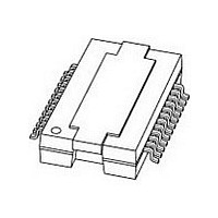
HSOP-26
Operational Class
Class-D
Audio Amplifier Output Configuration
1-Channel Mono/2-Channel Stereo
Output Power (typ)
160x1@8Ohm/80x2@4OhmW
Audio Amplifier Function
Speaker
Total Harmonic Distortion
0.15@8Ohm@1W%
Single Supply Voltage (typ)
Not RequiredV
Dual Supply Voltage (typ)
±27V
Power Supply Requirement
Dual
Rail/rail I/o Type
No
Single Supply Voltage (min)
Not RequiredV
Single Supply Voltage (max)
Not RequiredV
Dual Supply Voltage (min)
±14V
Dual Supply Voltage (max)
±29V
Operating Temp Range
-40C to 85C
Operating Temperature Classification
Industrial
Mounting
Surface Mount
Pin Count
24
Package Type
HSOP
Lead Free Status / RoHS Status
Lead free / RoHS Compliant
Other names
TDF8590TH/N1,118


NXP Semiconductors
17. Contents
1
2
3
4
5
5.1
5.2
6
6.1
6.2
6.3
6.4
6.4.1
6.4.2
6.4.3
6.4.4
6.4.5
6.5
6.6
7
8
9
10
10.1
10.2
11
12
12.1
12.2
12.3
12.4
12.5
12.6
12.7
12.8
13
14
15
15.1
15.2
15.3
15.4
16
17
General description . . . . . . . . . . . . . . . . . . . . . . 1
Features . . . . . . . . . . . . . . . . . . . . . . . . . . . . . . . 1
Ordering information . . . . . . . . . . . . . . . . . . . . . 1
Block diagram . . . . . . . . . . . . . . . . . . . . . . . . . . 2
Pinning information . . . . . . . . . . . . . . . . . . . . . . 2
Functional description . . . . . . . . . . . . . . . . . . . 3
Limiting values. . . . . . . . . . . . . . . . . . . . . . . . . 10
Thermal characteristics. . . . . . . . . . . . . . . . . . 11
Static characteristics. . . . . . . . . . . . . . . . . . . . 11
Dynamic characteristics . . . . . . . . . . . . . . . . . 13
Switching characteristics . . . . . . . . . . . . . . . . 15
Application information. . . . . . . . . . . . . . . . . . 15
Package outline . . . . . . . . . . . . . . . . . . . . . . . . 27
Revision history . . . . . . . . . . . . . . . . . . . . . . . . 28
Legal information. . . . . . . . . . . . . . . . . . . . . . . 29
Contact information. . . . . . . . . . . . . . . . . . . . . 29
Contents . . . . . . . . . . . . . . . . . . . . . . . . . . . . . . 30
Pinning . . . . . . . . . . . . . . . . . . . . . . . . . . . . . . . 2
Pin description . . . . . . . . . . . . . . . . . . . . . . . . . 3
Introduction . . . . . . . . . . . . . . . . . . . . . . . . . . . . 3
Mode selection . . . . . . . . . . . . . . . . . . . . . . . . . 4
Pulse width modulation frequency . . . . . . . . . . 5
Protections . . . . . . . . . . . . . . . . . . . . . . . . . . . . 6
Thermal foldback . . . . . . . . . . . . . . . . . . . . . . . 6
Overtemperature protection . . . . . . . . . . . . . . . 6
Overcurrent protection . . . . . . . . . . . . . . . . . . . 6
Window protection . . . . . . . . . . . . . . . . . . . . . . 8
Supply voltage protections . . . . . . . . . . . . . . . . 8
Diagnostic output . . . . . . . . . . . . . . . . . . . . . . . 9
Differential inputs . . . . . . . . . . . . . . . . . . . . . . . 9
Dynamic characteristics (SE) . . . . . . . . . . . . . 13
Dynamic characteristics (BTL) . . . . . . . . . . . . 14
BTL application . . . . . . . . . . . . . . . . . . . . . . . . 15
Output power estimation. . . . . . . . . . . . . . . . . 15
External clock . . . . . . . . . . . . . . . . . . . . . . . . . 16
Noise. . . . . . . . . . . . . . . . . . . . . . . . . . . . . . . . 16
Heat sink requirements. . . . . . . . . . . . . . . . . . 17
Pumping effects . . . . . . . . . . . . . . . . . . . . . . . 17
Application schematics . . . . . . . . . . . . . . . . . . 18
Curves measured in reference design . . . . . . 21
Data sheet status . . . . . . . . . . . . . . . . . . . . . . 29
Definitions . . . . . . . . . . . . . . . . . . . . . . . . . . . . 29
Disclaimers . . . . . . . . . . . . . . . . . . . . . . . . . . . 29
Trademarks . . . . . . . . . . . . . . . . . . . . . . . . . . . 29
2
80 W SE (4 ) or 1
Please be aware that important notices concerning this document and the product(s)
described herein, have been included in section ‘Legal information’.
© NXP B.V. 2007.
For more information, please visit: http://www.nxp.com
For sales office addresses, please send an email to: salesaddresses@nxp.com
160 W BTL (8 ) class-D amplifier
TDF8590TH
Document identifier: TDF8590TH_2
Date of release: 23 April 2007
All rights reserved.
Related parts for TDF8590TH/N1-T
Image
Part Number
Description
Manufacturer
Datasheet
Request
R

Part Number:
Description:
The TDF8590TH is a high-efficiency class-D audio power amplifier with low powerdissipation for application in car audio systems
Manufacturer:
NXP Semiconductors
Datasheet:

Part Number:
Description:
Tdf8590th 2 X 80 W Se 4 Ohm Or 1 X 160 W Btl 8 Ohm Class-d Amplifier
Manufacturer:
NXP Semiconductors
Datasheet:

Part Number:
Description:
IC AMP AUDIO PWR 160W D 24HSOP
Manufacturer:
NXP Semiconductors
Datasheet:
Part Number:
Description:
IC PWR AMP AUDIO CLASS D 24HSOP
Manufacturer:
NXP Semiconductors
Datasheet:

Part Number:
Description:
Manufacturer:
NXP Semiconductors
Datasheet:
Part Number:
Description:
NXP Semiconductors designed the LPC2420/2460 microcontroller around a 16-bit/32-bitARM7TDMI-S CPU core with real-time debug interfaces that include both JTAG andembedded trace
Manufacturer:
NXP Semiconductors
Datasheet:

Part Number:
Description:
NXP Semiconductors designed the LPC2458 microcontroller around a 16-bit/32-bitARM7TDMI-S CPU core with real-time debug interfaces that include both JTAG andembedded trace
Manufacturer:
NXP Semiconductors
Datasheet:
Part Number:
Description:
NXP Semiconductors designed the LPC2468 microcontroller around a 16-bit/32-bitARM7TDMI-S CPU core with real-time debug interfaces that include both JTAG andembedded trace
Manufacturer:
NXP Semiconductors
Datasheet:
Part Number:
Description:
NXP Semiconductors designed the LPC2470 microcontroller, powered by theARM7TDMI-S core, to be a highly integrated microcontroller for a wide range ofapplications that require advanced communications and high quality graphic displays
Manufacturer:
NXP Semiconductors
Datasheet:
Part Number:
Description:
NXP Semiconductors designed the LPC2478 microcontroller, powered by theARM7TDMI-S core, to be a highly integrated microcontroller for a wide range ofapplications that require advanced communications and high quality graphic displays
Manufacturer:
NXP Semiconductors
Datasheet:
Part Number:
Description:
The Philips Semiconductors XA (eXtended Architecture) family of 16-bit single-chip microcontrollers is powerful enough to easily handle the requirements of high performance embedded applications, yet inexpensive enough to compete in the market for hi
Manufacturer:
NXP Semiconductors
Datasheet:
Part Number:
Description:
The XA-S3 device is a member of Philips Semiconductors? XA(eXtended Architecture) family of high performance 16-bitsingle-chip microcontrollers
Manufacturer:
NXP Semiconductors
Datasheet:

Part Number:
Description:
The NXP BlueStreak LH75401/LH75411 family consists of two low-cost 16/32-bit System-on-Chip (SoC) devices
Manufacturer:
NXP Semiconductors
Datasheet:
Part Number:
Description:
The NXP LPC3130/3131 combine an 180 MHz ARM926EJ-S CPU core, high-speed USB2
Manufacturer:
NXP Semiconductors
Datasheet: