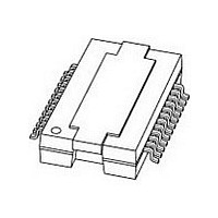
TDF8590TH/N1-T NXP Semiconductors, TDF8590TH/N1-T Datasheet - Page 5

TDF8590TH/N1-T
Manufacturer Part Number
TDF8590TH/N1-T
Description
Audio Amplifiers AMPLIFIER CLASS D
Manufacturer
NXP Semiconductors
Datasheet
1.TDF8590THN1-T.pdf
(30 pages)
Specifications of TDF8590TH/N1-T
Product
Class-D
Output Power
160 W
Available Set Gain
32 dB
Common Mode Rejection Ratio (min)
75 dB
Thd Plus Noise
0.15 %
Maximum Operating Temperature
+ 85 C
Mounting Style
SMD/SMT
Audio Load Resistance
8 Ohms
Dual Supply Voltage
+/- 27 V
Input Signal Type
Differential
Minimum Operating Temperature
- 40 C
Output Signal Type
Differential, Single
Supply Type
Dual
Output Type
1-Channel Mono or 2-Channel Stereo
Package / Case
HSOP-26
Operational Class
Class-D
Audio Amplifier Output Configuration
1-Channel Mono/2-Channel Stereo
Output Power (typ)
160x1@8Ohm/80x2@4OhmW
Audio Amplifier Function
Speaker
Total Harmonic Distortion
0.15@8Ohm@1W%
Single Supply Voltage (typ)
Not RequiredV
Dual Supply Voltage (typ)
±27V
Power Supply Requirement
Dual
Rail/rail I/o Type
No
Single Supply Voltage (min)
Not RequiredV
Single Supply Voltage (max)
Not RequiredV
Dual Supply Voltage (min)
±14V
Dual Supply Voltage (max)
±29V
Operating Temp Range
-40C to 85C
Operating Temperature Classification
Industrial
Mounting
Surface Mount
Pin Count
24
Package Type
HSOP
Lead Free Status / RoHS Status
Lead free / RoHS Compliant
Other names
TDF8590TH/N1,118
NXP Semiconductors
TDF8590TH_2
Product data sheet
6.3 Pulse width modulation frequency
The value of the RC time constant should be dimensioned for 500 ms. If the 100 F
capacitor is left out of the application the voltage on pin MODE will be applied with a much
smaller time constant, which might result in audible pop noises during start-up (depending
on DC output offset voltage and used loudspeaker).
In order to fully charge the coupling capacitors at the inputs, the amplifier will remain
automatically in Mute mode for approximately 150 ms before switching to Operating
mode. A complete overview of the start-up timing is given in
The output signal of the amplifier is a PWM signal with a switching frequency that is set by
an external resistor R
for the carrier frequency is between 300 kHz and 350 kHz. An external resistor R
30 k sets the frequency to 310 kHz.
Fig 4. Timing on mode selection input
0 V (SGND)
0 V (SGND)
V
V
MODE
2.5 V
MODE
5 V
5 V
ext(OSC)
Rev. 02 — 23 April 2007
standby
standby
2
connected between pins OSC and V
80 W SE (4 ) or 1
100 ms
100 ms
mute
50 ms
50 ms
160 W BTL (8 ) class-D amplifier
Figure
switching
operating
switching
operating
audio
audio
TDF8590TH
SSA
4.
001aad837
. An optimum setting
time
time
© NXP B.V. 2007. All rights reserved.
ext(OSC)
5 of 30
of


