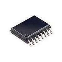
TDA8543TD-T NXP Semiconductors, TDA8543TD-T Datasheet - Page 4

TDA8543TD-T
Manufacturer Part Number
TDA8543TD-T
Description
Audio Amplifiers 1.4W BTL AUDIO AMP
Manufacturer
NXP Semiconductors
Datasheet
1.TDA8543TN1518.pdf
(19 pages)
Specifications of TDA8543TD-T
Product
Class-AB
Output Power
2.2 W
Available Set Gain
30 dB
Thd Plus Noise
0.15 %
Operating Supply Voltage
5 V
Maximum Power Dissipation
1200 mW
Maximum Operating Temperature
+ 85 C
Mounting Style
SMD/SMT
Audio Load Resistance
16 Ohms
Input Bias Current (max)
0.5 uA
Input Signal Type
Differential or Single
Minimum Operating Temperature
- 40 C
Output Signal Type
Differential, Single
Supply Type
Single
Supply Voltage (max)
18 V
Supply Voltage (min)
2.2 V
Output Type
1-Channel Mono
Package / Case
SOT-109
Lead Free Status / RoHS Status
Lead free / RoHS Compliant
Other names
TDA8543T/N1,518
NXP Semiconductors
FUNCTIONAL DESCRIPTION
The TDA8543(T) is a BTL audio power amplifier capable
of delivering an output power between 1 and 2 W,
depending on supply voltage, load resistance
and package. Using the MODE pin the device can
be switched to standby and mute condition. The device
is protected by an internal thermal shutdown protection
mechanism.
The gain can be set within a range from 6 dB to 30 dB
by external feedback resistors.
Power amplifier
The power amplifier is a Bridge Tied Load (BTL) amplifier
with a complementary PNP-NPN output stage.
LIMITING VALUES
In accordance with the Absolute Maximum Rating System (IEC 134).
QUALITY SPECIFICATION
In accordance with “SNW-FQ-611-E”. The number of the quality specification can be found in the “Quality Reference
Handbook”. The handbook can be ordered using the code 9397 750 00192.
THERMAL CHARACTERISTICS
1997 Jun 12
V
V
I
T
T
V
P
R
ORM
stg
amb
CC
I
psc
tot
2 W BTL audio amplifier
th j-a
SYMBOL
SYMBOL
thermal resistance from junction to ambient
supply voltage
input voltage
repetitive peak output current
storage temperature
operating ambient temperature
AC and DC short-circuit safe voltage
total power dissipation
TDA8543T (SO16)
TDA8543 (DIP16)
PARAMETER
PARAMETER
4
The voltage loss on the positive supply line is
the saturation voltage of a PNP power transistor,
on the negative side the saturation voltage of an
NPN power transistor.
Mode select pin
The device is in standby mode (with a very low current
consumption) if the voltage at the MODE
pin is >(V
voltage level of less than 0.5 V the amplifier is fully
operational.
In the range between 1.5 V and V
is in mute condition. The mute condition is useful to
suppress plop noise at the output, caused by charging of
the input capacitor.
operating
non-operating
SO16
DIP16
CONDITIONS
in free air
CC
CONDITIONS
− 0.5 V), or if this pin is floating. At a MODE
−0.3
−0.3
−
−55
−40
−
−
−
MIN.
+18
V
1
+150
+85
10
1.2
2.2
CC
CC
VALUE
MAX.
− 1.5 V the amplifier
100
Product specification
55
+ 0.3
TDA8543
V
V
A
°C
°C
V
W
W
UNIT
UNIT
K/W
K/W


