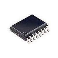
TDA8543TD-T NXP Semiconductors, TDA8543TD-T Datasheet - Page 7

TDA8543TD-T
Manufacturer Part Number
TDA8543TD-T
Description
Audio Amplifiers 1.4W BTL AUDIO AMP
Manufacturer
NXP Semiconductors
Datasheet
1.TDA8543TN1518.pdf
(19 pages)
Specifications of TDA8543TD-T
Product
Class-AB
Output Power
2.2 W
Available Set Gain
30 dB
Thd Plus Noise
0.15 %
Operating Supply Voltage
5 V
Maximum Power Dissipation
1200 mW
Maximum Operating Temperature
+ 85 C
Mounting Style
SMD/SMT
Audio Load Resistance
16 Ohms
Input Bias Current (max)
0.5 uA
Input Signal Type
Differential or Single
Minimum Operating Temperature
- 40 C
Output Signal Type
Differential, Single
Supply Type
Single
Supply Voltage (max)
18 V
Supply Voltage (min)
2.2 V
Output Type
1-Channel Mono
Package / Case
SOT-109
Lead Free Status / RoHS Status
Lead free / RoHS Compliant
Other names
TDA8543T/N1,518
NXP Semiconductors
Notes to the AC characteristics
1. Gain of the amplifier is
2. The noise output voltage is measured at the output in a frequency range from 20 Hz to 20 kHz (unweighted), with
3. Supply voltage ripple rejection is measured at the output, with a source impedance of R
4. Supply voltage ripple rejection is measured at the output, with a source impedance of R
5. Output voltage in mute position is measured with an input voltage of 1 V (RMS) in a bandwidth of 20 kHz, so including
TEST AND APPLICATION INFORMATION
Test conditions
Because the application can be either Bridge Tied Load
(BTL) or Single-Ended (SE), the curves of each application
are shown separately.
The thermal resistance = 55 K/W for the DIP16 envelope;
the maximum sine wave power dissipation
for T
For T
See the power derating curve illustrated in Fig.3.
BTL application
T
f = 1 kHz, R
22 Hz to 22 kHz.
The BTL application diagram is shown in Fig.4.
The quiescent current has been measured without
any load impedance. The total harmonic distortion
as a function of frequency was measured with a low-pass
filter of 80 kHz. The value of capacitor C2 influences
the behaviour of the SVRR at low frequencies, increasing
the value of C2 increases the performance of the SVRR.
The figure of the mode select voltage (V
of the supply voltage shows three areas; operating, mute
and standby. It shows, that the DC-switching levels
of the mute and standby respectively depends
on the supply voltage level.
1997 Jun 12
150 25
--------------------- -
150 60
--------------------- -
amb
2 W BTL audio amplifier
55
55
a source impedance of R
The ripple voltage is a sine wave with a frequency of 1 kHz and an amplitude of 100 mV (RMS), which is applied
to the positive supply rail.
The ripple voltage is a sine wave with a frequency between 100 Hz and 20 kHz and an amplitude of 100 mV (RMS),
which is applied to the positive supply rail.
noise.
amb
–
–
= 25 °C if not specially mentioned, V
amb
= 25 °C is:
= 60 °C the maximum total power dissipation is:
=
=
L
2.27 W
1.63 W
= 8 Ω, G
v
= 20 dB, audio band-pass
2
S
×
= 0 Ω at the input.
R2
------- -
R1
in test circuit of Fig.4.
ms
CC
) as a function
= 5 V,
7
SE application
T
f = 1 kHz, R
22 Hz to 22 kHz.
The SE application diagram is shown in Fig.14.
The capacitor value of C3 in combination with the load
impedance determines the low frequency behaviour.
The total harmonic distortion as a function of frequency
was measured with low-pass filter of 80 kHz. The value
of capacitor C2 influences the behaviour of the SVRR
at low frequencies, increasing the value of C2 increases
the performance of the SVRR.
General remark
The frequency characteristic can be adapted
by connecting a small capacitor across the feedback
resistor. To improve the immunity of HF radiation in radio
circuit applications, a small capacitor can be connected
in parallel with the feedback resistor; this creates a
low-pass filter.
amb
= 25 °C if not specially mentioned, V
L
= 4 Ω, G
v
= 20 dB, audio band-pass
S
S
= 0 Ω at the input.
= 0 Ω at the input.
Product specification
TDA8543
CC
= 7.5 V,


