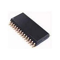
UDA1344TSDB NXP Semiconductors, UDA1344TSDB Datasheet - Page 7

UDA1344TSDB
Manufacturer Part Number
UDA1344TSDB
Description
Audio CODECs AUDIO CODEC W/DSP
Manufacturer
NXP Semiconductors
Datasheet
1.UDA1344TSN2512.pdf
(27 pages)
Specifications of UDA1344TSDB
Number Of Adc Inputs
2
Number Of Dac Outputs
2
Conversion Rate
55 KSPs
Interface Type
Serial (I2S), L3
Resolution
20 bit
Operating Supply Voltage
2.7 V to 3.6 V
Maximum Operating Temperature
+ 85 C
Mounting Style
SMD/SMT
Package / Case
SSOP-28
Minimum Operating Temperature
- 40 C
Number Of Channels
2 ADC, 2 DAC
Snr
100 dB
Supply Current
9 mA
Lead Free Status / RoHS Status
Lead free / RoHS Compliant
Other names
UDA1344TS/N2,512
NXP Semiconductors
Mute (ADC)
On recovery from power-down or switching on of the
system clock, the serial data output on pin DATAO is held
at LOW level until valid data is available from the
decimation filter. This time depends on whether the
DC-cancellation filter is selected:
• DC cancel off:
• DC cancel on:
Interpolation filter (DAC)
The digital filter interpolates from 1f
a cascade of a recursive filter and an FIR filter.
Table 4 Interpolation filter characteristics
Noise shaper (DAC)
The 3rd-order noise shaper operates at 128f
in-band quantization noise to frequencies well above the
audio band. This noise shaping technique enables high
signal-to-noise ratios to be achieved. The noise shaper
output is converted into an analog signal using a Filter
Stream Digital-to-Analog Converter (FSDAC).
Filter stream DAC
The FSDAC is a semi-digital reconstruction filter that
converts the 1-bit data stream of the noise shaper to an
analog output voltage. The filter coefficients are
implemented as current sources and are summed at virtual
ground of the output operational amplifier. In this way very
high signal-to-noise performance and low clock jitter
sensitivity is achieved. A post-filter is not needed due to
the inherent filter function of the DAC. On-board amplifiers
convert the FSDAC output current to an output voltage
signal capable of driving a line output.
The output voltage of the FSDAC scales proportionally
with the power supply voltage.
2001 Jun 29
Pass-band ripple
Stop band
Dynamic range
Gain
Low-voltage low-power stereo audio
CODEC with DSP features
t
t
=
=
1024
------------ -
12288
--------------- -
ITEM
f
f
s
s
; t = 23.2 ms at f
; t = 279 ms at f
CONDITIONS
0 − 0.45f
0 − 0.45f
>0.55f
DC
s
s
= 44.1 kHz
= 44.1 kHz.
s
s
s
s
to 128f
VALUE (dB)
s
s
by means of
±0.03
. It shifts
−3.5
−50
108
7
Multiple format input/output interface
The UDA1344TS supports the following data input/output
formats:
• I
• MSB-justified serial format with data word length of up to
• LSB-justified serial format with data word lengths of
• Combined data formats:
The formats are illustrated in Fig.3. Left and right
data-channel words are time multiplexed.
Control mode selection
The UDA1344TS can be used under L3 microcontroller
interface control or static pin control. The mode can be set
via the mode control pins MC1 and MC2 (see Table 5).
Table 5 Mode control pins
Important: in the L3 mode the UDA1344TS is completely
pin and function compatible with the UDA1340M.
20 bits
16, 18 or 20 bits (in L3 mode only)
– L3 mode: MSB-justified data output and
– Static pin mode: MSB-justified data output and
2
S-bus format with data word length of up to 20 bits
PIN MC2
LSB-justified 16, 18 and 20 bits data input
LSB-justified 16 and 20 bits data input.
HIGH
HIGH
LOW
LOW
PIN MC1
HIGH
HIGH
LOW
LOW
UDA1344TS
Product specification
L3 mode
Test mode
Static pin mode
MODE


