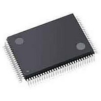
ISPPAC-CLK5520V-01T100I Lattice, ISPPAC-CLK5520V-01T100I Datasheet - Page 21

ISPPAC-CLK5520V-01T100I
Manufacturer Part Number
ISPPAC-CLK5520V-01T100I
Description
Clock Drivers & Distribution PROGRAMMABLE CLOCK GENERATOR
Manufacturer
Lattice
Datasheet
1.PAC-SYSTEMCLK5520.pdf
(48 pages)
Specifications of ISPPAC-CLK5520V-01T100I
Minimum Operating Temperature
- 40 C
Mounting Style
SMD/SMT
Maximum Operating Temperature
85 C
Package / Case
TQFP-100
Lead Free Status / RoHS Status
Lead free / RoHS Compliant
Available stocks
Company
Part Number
Manufacturer
Quantity
Price
Company:
Part Number:
ISPPAC-CLK5520V-01T100I
Manufacturer:
Lattice Semiconductor Corporation
Quantity:
10 000
Lattice Semiconductor
Clock reference inputs may be configured to interface to signals from the following logic families with little or no
external support circuitry:
Each input also features internal programmable termination resistors, as shown in Figure 16.
Figure 16. ispClock5500 Clock Reference Input Structure (REFA+/- Pair Shown)
The following usage guidelines are suggested for interfacing to supported logic families.
LVTTL (3.3V), LVCMOS (1.8V, 2.5V, 3.3V)
The receiver should be set to LVCMOS or LVTTL mode, and the input signal should be connected to the ‘+’ termi-
nal of the input pair (e.g. REFA+). The ‘-’ input terminal should be left floating. CMOS transmission lines are gener-
ally source terminated, so all termination resistors should be set to the OPEN state. Figure 17 shows the proper
configuration. Please note that because switching thresholds are different for LVCMOS running at 1.8V, there is a
separate configuration setting for this particular standard.
• LVTTL (3.3V)
• LVCMOS (1.8V, 2.5V, 3.3V)
• SSTL2
• SSTL3
• HSTL
• LVDS
• LVPECL (differential, 3.3V)
REFVTT
REFA+
REFA-
ispClock5500
R
T
R
T
Single-ended
Differential
21
Receiver
Receiver
ispClock5500 Family Data Sheet
To Internal
Logic


