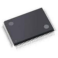
ISPPAC-CLK5520V-01T100I Lattice, ISPPAC-CLK5520V-01T100I Datasheet - Page 33

ISPPAC-CLK5520V-01T100I
Manufacturer Part Number
ISPPAC-CLK5520V-01T100I
Description
Clock Drivers & Distribution PROGRAMMABLE CLOCK GENERATOR
Manufacturer
Lattice
Datasheet
1.PAC-SYSTEMCLK5520.pdf
(48 pages)
Specifications of ISPPAC-CLK5520V-01T100I
Minimum Operating Temperature
- 40 C
Mounting Style
SMD/SMT
Maximum Operating Temperature
85 C
Package / Case
TQFP-100
Lead Free Status / RoHS Status
Lead free / RoHS Compliant
Available stocks
Company
Part Number
Manufacturer
Quantity
Price
Company:
Part Number:
ISPPAC-CLK5520V-01T100I
Manufacturer:
Lattice Semiconductor Corporation
Quantity:
10 000
Lattice Semiconductor
If any of the above items are modified, the change will apply across all profiles. In some cases this may cause
unanticipated behavior. If multiple profiles are used in a design, the suitability of the profile independent settings
must be considered with respect to each of the individual profiles.
When a profile is changed by modifying the values of the PS0 and PS1 inputs, it is necessary to assert a RESET
signal to the ispClock5500 to restart the PLL and resynchronize all the internal dividers.
RESET and Power-up Functions
To ensure proper PLL startup and synchronization of outputs, the ispClock5500 provides both internally generated
and user-controllable external reset signals. An internal reset is generated whenever the device is powered up. An
external reset may be applied by asserting a logic HIGH at the RESET pin. Please note that the RESET pin does
not have an internal pull-up or pull-down resistor associated with it and should be tied LOW if not used. Asserting
RESET resets all internal dividers, and will cause the PLL to lose lock. On losing lock, the VCO frequency will begin
dropping. The length of time required to regain lock is related to the length of time for which RESET was asserted.
Output phase relationships among the outputs may not be valid until the ispClock5500 asserts its LOCK output.
When the ispClock5500 begins operating from initial power-on, the VCO starts running at a very low frequency
(<100 MHz) which gradually increases as it approaches a locked condition. To prevent invalid outputs from being
applied to the rest of the system, it is recommended that either the SGATE, OEX, or OEY pins be used to control
the outputs based on the status of the LOCK pin. Holding the SGATE pin LOW during power-up will result in the
BANK outputs being asserted HIGH or LOW (depending on inversion status) until SGATE is brought HIGH. Assert-
ing OEX or OEY high will result in the BANK outputs being held in a high-impedance state until the OEX or OEY
pin is pulled LOW. One should not use the GOE pin to control the outputs in anticipation of LOCK status, as holding
GOE HIGH also disables internal feedback and will prevent the device from ever achieving lock.
Software-Based Design Environment
Designers can configure the ispClock5500 using Lattice’s PAC-Designer software, an easy to use, Microsoft Windows
compatible program. Circuit designs are entered graphically and then verified, all within the PAC-Designer environ-
ment. Full device programming is supported using PC parallel port I/O operations and a download cable connected to
the serial programming interface pins of the ispClock5500. A library of configurations is included with basic solutions
and examples of advanced circuit techniques are available on the Lattice web site at www.latticesemi.com. In addi-
tion, comprehensive on-line and printed documentation is provided that covers all aspects of PAC-Designer operation.
The PAC-Designer schematic window, shown in Figure 30 provides access to all configurable ispClock5500 elements
via its graphical user interface. All analog input and output pins are represented. Static or non-configurable pins such
as power, ground and the serial digital interface are omitted for clarity. Any element in the schematic window can be
accessed via mouse operations as well as menu commands. When completed, configurations can be saved and
downloaded to devices.
• V-Divider to be used as feedback source
• Internal feedback delay compensation
• Fine/Coarse skew mode selection
• UES string
– Signal Inversion
33
ispClock5500 Family Data Sheet


