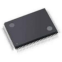
ISPPAC-CLK5520V-01T100I Lattice, ISPPAC-CLK5520V-01T100I Datasheet - Page 24

ISPPAC-CLK5520V-01T100I
Manufacturer Part Number
ISPPAC-CLK5520V-01T100I
Description
Clock Drivers & Distribution PROGRAMMABLE CLOCK GENERATOR
Manufacturer
Lattice
Datasheet
1.PAC-SYSTEMCLK5520.pdf
(48 pages)
Specifications of ISPPAC-CLK5520V-01T100I
Minimum Operating Temperature
- 40 C
Mounting Style
SMD/SMT
Maximum Operating Temperature
85 C
Package / Case
TQFP-100
Lead Free Status / RoHS Status
Lead free / RoHS Compliant
Available stocks
Company
Part Number
Manufacturer
Quantity
Price
Company:
Part Number:
ISPPAC-CLK5520V-01T100I
Manufacturer:
Lattice Semiconductor Corporation
Quantity:
10 000
Lattice Semiconductor
ispClock5500 Family Data Sheet
Note that while a floating 100Ω resistor forms a complete termination for an LVDS signal line, additional circuitry
may be required to satisfactorily terminate a differential LVPECL signal. This is because a true bipolar LVPECL out-
put driver typically requires an external DC ‘pull-down’ path to a V
termination voltage (typically VCC-2V) to
TERM
properly bias its open emitter output stage. When interfacing to an LVPECL input signal, the ispClock5500’s inter-
nal termination resistors should not be used for this pull-down function, as they may be damaged from excessive
current. The pull-down should be implemented with external resistors placed close to the LVPECL driver
(Figure 21)
Figure 21. LVPECL Input Receiver Configuration
ispClock5500
Differential
+Signal In
Receiver
REFA+
LVPECL
Driver
-Signal In
REFA-
R
R
50
50
PD
PD
CLOSED
CLOSED
V
No Connect
TERM
REFVTT
Please note that while the above discussions specify using 50Ω termination impedances, the actual impedance
required to properly terminate the transmission line and maintain good signal integrity may vary from this ideal. The
actual impedance required will be a function of the driver used to generate the signal and the transmission medium
used (PCB traces, connectors and cabling). The ispClock5500’s ability to adjust input impedance over a range of
40Ω to 70Ω allows the user to adapt his circuit to non-ideal behaviors from the rest of the system without having to
swap out components.
Output Drivers
The ispClock5500 provide banks of configurable, internally-terminated high-speed dual-output line drivers. The
ispClock5510 provides five driver banks, while the ispClock5520 provides ten. Each of these driver banks may be
configured to provide either a single differential output signal, or a pair of single-ended output signals. Programma-
ble internal source-series termination allows the ispClock5500 to be matched to transmission lines with imped-
2
ances ranging from 40 to 70 Ohms. The outputs may be independently enabled or disabled, either from E
CMOS
configuration or by external control lines. Additionally, each can be independently programmed to provide a fixed
amount of signal delay or skew, allowing the user to compensate for the effects of unequal PCB trace lengths or
loading effects. Figure 22 shows a block diagram of a typical ispClock5500 output driver bank and associated skew
control.
Because of the high edge rates which can be generated by the ispClock5500’s clock output drivers, the VCCO
power supply pin for each output bank should be individually bypassed. Low ESR capacitors with values ranging
from 0.01 to 0.1 µF may be used for this purpose. Each bypass capacitor should be placed as close to its respec-
tive output bank power pins (VCCO and GNDO) pins as is possible to minimize interconnect length and associated
parasitic inductances.
24


