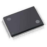
ISPPAC-CLK5510V-01T48C Lattice, ISPPAC-CLK5510V-01T48C Datasheet - Page 15

ISPPAC-CLK5510V-01T48C
Manufacturer Part Number
ISPPAC-CLK5510V-01T48C
Description
Clock Drivers & Distribution PROGRAMMABLE CLOCK GENERATOR
Manufacturer
Lattice
Datasheet
1.PAC-SYSTEMCLK5520.pdf
(48 pages)
Specifications of ISPPAC-CLK5510V-01T48C
Minimum Operating Temperature
0 C
Mounting Style
SMD/SMT
Maximum Operating Temperature
70 C
Package / Case
TQFP-100
Lead Free Status / RoHS Status
Lead free / RoHS Compliant
Available stocks
Company
Part Number
Manufacturer
Quantity
Price
Company:
Part Number:
ISPPAC-CLK5510V-01T48C
Manufacturer:
Lattice Semiconductor Corporation
Quantity:
10 000
Lattice Semiconductor
Typical Performance Characteristics (Cont.)
Detailed Description
PLL Subsystem
The ispClock5500 provides an integrated phase-locked-loop (PLL) which may be used to generate output clock
signals at lower, higher, or the same frequency as a user-supplied input reference signal. The core functions of the
PLL are an edge-sensitive phase detector, a programmable loop filter, and a high-speed voltage-controlled oscilla-
tor (VCO). Additionally, a set of programmable input, output and feedback dividers (M, N, V[1..5]) is provided to
support the synthesis of different output frequencies.
Phase/Frequency Detector
The ispClock5500 provides an edge-sensitive phase/frequency detector (PFD), which means that the device will
function properly over a wide range of input clock reference duty cycles. It is only necessary that the input refer-
ence clock meet specified minimum HIGH and LOW times (t
PFD. The PFD’s output is of a classical charge-pump type, outputting charge packets which are then integrated by
the PLL‘s loop filter.
A lock-detection feature is also associated with the PFD. When the ispClock5500 is in a LOCKED state, the LOCK
output pin goes LOW. The lock detector has two operating modes; phase lock mode and frequency lock mode. In
phase-lock mode, the LOCK signal is asserted if the phases of the reference and feedback signals match, whereas
in frequency-lock mode the LOCK signal is asserted when the frequencies of the feedback and reference signals
match. The option of which mode to use is programmable and may be set using PAC-Designer software (available
from Lattice’s web site at www.latticesemi.com).
In phase-lock mode the lock detector asserts the LOCK signal as soon as a lock condition is determined. In fre-
quency-lock mode, however, the PLL must be in a locked condition for a set number of phase detector cycles
before the LOCK signal will be asserted. The number of cycles required before asserting the LOCK signal in fre-
quency-lock mode can be set from 16 through 256, in increments of 16.
The LOCK signal is generated in response to certain phase or frequency matches being detected at the input of
the phase-frequency detector. Therefore it is possible that the LOCK signal may be asserted before the PLL has
completely stabilized, and may change state while the PLL is in the process of stabilizing. Additionally, the output
dividers are resynchronized in response to the frequency lock detector detecting a lock condition, even when the
lock detector is set to phase mode. The frequency lock detector and phase lock detector are completely indepen-
dent circuits.
Because the frequency lock detector requires a user-selectable number of cycles (16-256) to determine a lock con-
dition, it is possible for the dividers to experience a resynchronization event a short time after a phase lock condi-
tion is detected. This may result in an glitch or missing clock cycle on one or more of the outputs. For all of the
120
100
80
60
40
20
0
300
V = 4
Typical Period Jitter vs. VCO Frequency
350
V = 8
V = 16
400
VCO Frequency (MHz)
PFD = 80 MHz
V = 32
450
15
500
CLOCKHI,
550
600
t
CLOCKLO
ispClock5500 Family Data Sheet
650
) for it to properly recognized by the
700


