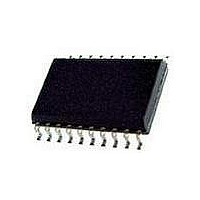
PCK3807ADB NXP Semiconductors, PCK3807ADB Datasheet - Page 3

PCK3807ADB
Manufacturer Part Number
PCK3807ADB
Description
Clock Buffer 1:10 LVTTL CLK DISTR DEVICE
Manufacturer
NXP Semiconductors
Datasheet
1.PCK3807APW118.pdf
(13 pages)
Specifications of PCK3807ADB
Number Of Outputs
10
Max Input Freq
150 MHz
Propagation Delay (max)
4.5 ns, 4 ns
Supply Voltage (max)
3.6 V
Supply Voltage (min)
2.3 V
Maximum Operating Temperature
+ 85 C
Minimum Operating Temperature
- 40 C
Mounting Style
SMD/SMT
Package / Case
SSOP-20
Operating Supply Voltage (max)
3.6V
Operating Temp Range
-40C to 85C
Propagation Delay Time
4.5ns
Operating Supply Voltage (min)
2.3V
Mounting
Surface Mount
Pin Count
20
Operating Supply Voltage (typ)
2.5/3.3V
Package Type
SSOP
Quiescent Current
10uA
Input Frequency
150MHz
Operating Temperature Classification
Industrial
Lead Free Status / RoHS Status
Lead free / RoHS Compliant
Other names
PCK3807ADB,112
Available stocks
Company
Part Number
Manufacturer
Quantity
Price
Company:
Part Number:
PCK3807ADB
Manufacturer:
TI
Quantity:
300
1. Stresses greater than those listed under ABSOLUTE MAXIMUM RATINGS may cause permanent damage to the device. This is a stress
2. V
3. Input terminal.
4. Outputs terminals.
1. This parameter is measured at characterization but not tested.
Philips Semiconductors
ABSOLUTE MAXIMUM RATINGS
NOTES:
CAPACITANCE
T
NOTE:
RECOMMENDED OPERATING CONDITIONS
2004 Aug 27
SYMBOL
V
V
V
T
I
amb
SYMBOL
C
C
O
SYMBOL
SYMBOL
stg
TERM
TERM
TERM
1:10 LVTTL clock distribution device
i
o
rating only and functional operation of the device at these or any other conditions above those indicated in the operational sections of this
specification is not implied. Exposure to absolute maximum rating conditions for extended periods may affect reliability.
T
V
CC
= +25 C, f = 1.0 MHz
C
f
amb
CC
IN
L
2
3
4
terminals.
CURRENT
DYNAMIC
I
DD
DC supply voltage
Input signal frequency
Operating free-air temperature range
Output capacitance load
(mA)
PARAMETER
Input capacitance
Output capacitance
DESCRIPTION
Terminal voltage with respect to GND
Terminal voltage with respect to GND
Terminal voltage with respect to GND
Storage temperature
DC output current
160
140
120
100
80
60
40
20
0
0
Figure 1. Dynamic current vs. clock frequency, V
1
PARAMETER
PARAMETER
50
CLOCK FREQUENCY (MHz)
CONDITIONS
V
V
IN
OUT
3
= 0 V
= 0 V
100
CC
= 3.3 V
MIN
–0.5
–0.5
–0.5
–65
–60
150
TYP
2.5
5.5
MIN
–40
2.3
LOAD = 15 pF AND 33
LOAD = 0
0
–
LIMITS
MAX
+4.6
+7
V
+150
+60
CC
MAX
4
6
+0.5
PCK3807A
MAX
150
+85
3.6
50
Product data sheet
200
UNIT
pF
pF
SW02071
UNIT
V
V
V
mA
C
UNIT
UNIT
MHz
pF
V
C


