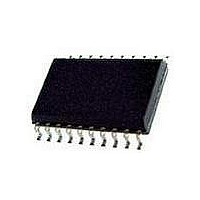
PCK3807ADB NXP Semiconductors, PCK3807ADB Datasheet - Page 5

PCK3807ADB
Manufacturer Part Number
PCK3807ADB
Description
Clock Buffer 1:10 LVTTL CLK DISTR DEVICE
Manufacturer
NXP Semiconductors
Datasheet
1.PCK3807APW118.pdf
(13 pages)
Specifications of PCK3807ADB
Number Of Outputs
10
Max Input Freq
150 MHz
Propagation Delay (max)
4.5 ns, 4 ns
Supply Voltage (max)
3.6 V
Supply Voltage (min)
2.3 V
Maximum Operating Temperature
+ 85 C
Minimum Operating Temperature
- 40 C
Mounting Style
SMD/SMT
Package / Case
SSOP-20
Operating Supply Voltage (max)
3.6V
Operating Temp Range
-40C to 85C
Propagation Delay Time
4.5ns
Operating Supply Voltage (min)
2.3V
Mounting
Surface Mount
Pin Count
20
Operating Supply Voltage (typ)
2.5/3.3V
Package Type
SSOP
Quiescent Current
10uA
Input Frequency
150MHz
Operating Temperature Classification
Industrial
Lead Free Status / RoHS Status
Lead free / RoHS Compliant
Other names
PCK3807ADB,112
Available stocks
Company
Part Number
Manufacturer
Quantity
Price
Company:
Part Number:
PCK3807ADB
Manufacturer:
TI
Quantity:
300
1. For conditions shown as Max or Min, use appropriate value specified under Electrical Characteristics for the applicable device type.
2. Typical values are at V
3. Duration of the test should not exceed one second.
4. Not more than one output shorted at one time. Duration of the test should not exceed one second.
5. This parameter is guaranteed but not tested.
6. V
Philips Semiconductors
DC ELECTRICAL CHARACTERISTICS OVER OPERATING RANGE
T
NOTES:
2004 Aug 27
amb
V
V
I
I
V
I
I
V
V
I
l
V
I
I
SYMBOL
IH
IL
ODH
ODL
OFF
OS
CCL
CCH
IH
IL
IK
OH
OL
hys
1:10 LVTTL clock distribution device
OH
= –40 C to +85 C, V
= V
CC
HIGH-level input voltage (Input pins)
HIGH-level input voltage (I/O pins)
LOW-level input voltage (Input pins)
LOW-level input voltage (I/O pins)
HIGH-level input current (Input pins)
HIGH-level input current (I/O pins)
LOW-level input current (Input pins)
LOW-level input current (I/O pins)
Clamp diode voltage
HIGH-level input current
LOW-level input current
HIGH-level output voltage
LOW-level output voltage
Input power off leakage
Short circuit current
Input hysteresis
Quiescent power supply current
– 0.6 V at rated current.
CC
PARAMETER
CC
= 3.3 V, +25 C ambient.
= 3.3 V
5
0.3 V, unless otherwise specified
V
V
V
V
V
V
V
V
V
V
V
V
V
V
V
V
V
V
–
V
V
CC
CC
CC
CC
CC
CC
CC
CC
CC
CC
CC
CC
CC
CC
CC
CC
CC
CC
CC
IN
= GND or V
= Max
= 3.0 V to 3.6 V
= 2.3 V to 2.7 V
= 3.0 V to 3.6 V
= 2.3 V to 2.7 V
= Max
= Max
= Min; I
= 3.3 V; V
= 3.3 V; V
= 2.3 V to 3.6 V
= 2.3 V
= 3.0 V
= 2.3 V to 3.6 V
= 2.3 V
= 3.0 V
= 3.0 V
= 0 V; V
= Max; V
TEST CONDITIONS
IN
IN
O
= –18 mA
IN
IN
= 4.5 V
CC
= GND
5
= V
= V
IH
IH
4
or V
or V
V
V
V
V
I
I
I
I
I
I
I
OH
OH
OH
OL
OL
OL
OL
I
I
I
I
= 5.5 V
= V
= GND
= GND
IL
IL
= 8 mA
= 16 mA
= 24 mA
= 0.1 mA
= –0.1 mA
= –8 mA
= –8 mA
; Vo =1.5 V
; Vo =1.5 V
CC
1
3
3
2
1.7
–0.5
–0.5
–
–
–
–
–
–36
50
V
1.9
2.4
–
–
–
–
–
0
–
–
CC
MIN
6
– 0.2
–
–
–
–
–
–
–
–
–0.7
–120
150
–
–
3
–
–
0.2
0.3
–
–155
150
0.1
TYP
PCK3807A
5.5
3.6
0.8
0.7
–1.0
–150
200
–
–
–
0.2
0.3
0.4
0.5
–240
–
10
1
1
1
1
1
MAX
Product data sheet
V
V
V
mA
mA
V
V
mA
mV
A
A
A
A
UNIT


