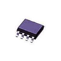
PCF8593TD NXP Semiconductors, PCF8593TD Datasheet - Page 13

PCF8593TD
Manufacturer Part Number
PCF8593TD
Description
Real Time Clock LO PWR CLOCK/CAL
Manufacturer
NXP Semiconductors
Datasheet
1.PCF8593P112.pdf
(35 pages)
Specifications of PCF8593TD
Function
Alarm, Timer Interrupt
Rtc Memory Size
8 B
Supply Voltage (max)
6 V
Supply Voltage (min)
1 V
Maximum Operating Temperature
+ 85 C
Minimum Operating Temperature
- 40 C
Mounting Style
SMD/SMT
Rtc Bus Interface
Serial
Package / Case
SOT-96
Time Format
HH:MM:SS:hh
Lead Free Status / RoHS Status
Lead free / RoHS Compliant
Other names
PCF8593T/1,112
NXP Semiconductors
PCF8593
Product data sheet
7.10.1 Designing
7.11 Initialization
In the 50 Hz clock mode or event-counter mode the oscillator is disabled and the oscillator
input is switched to a high-impedance state. This allows the user to feed the 50 Hz
reference frequency or an external high speed event signal into the input OSCI.
When designing the printed-circuit board layout, keep the oscillator components as close
to the IC package as possible, and keep all other signal lines as far away as possible. In
applications involving tight packing of components, shielding of the oscillator may be
necessary. AC coupling of extraneous signals can introduce oscillator inaccuracy.
Note that immediately following power-on, all internal registers are undefined and,
following a RESET pulse on pin 3, must be defined via software. Attention should be paid
to the possibility that the device may be initially in event-counter mode, in which event the
oscillator will not operate. Over-ride can be achieved via software.
Reset is accomplished by applying an external RESET pulse (active LOW) at pin 3. When
reset occurs only the I
clock counters are not affected by RESET. RESET must return HIGH during device
operation.
An RC combination can also be utilized to provide a power-on RESET signal at pin 3. In
this event, the values of the PCF8593 must fulfil the following relationship to guarantee
power-on reset (see
RESET input must be input must be ≤ 0.3V
It is recommended to set the stop counting flag of the control and status register before
loading the actual time into the counters. Loading of illegal states may lead to a temporary
clock malfunction.
Fig 13. PCF8593 reset
To avoid overload of the internal diode by falling V
to R
value will be V
R
if C
All information provided in this document is subject to legal disclaimers.
R
≥ 0.2 μF. Note that RC must be evaluated with the actual V
Figure
DD
2
Rev. 04 — 6 October 2010
C-bus interface is reset. The control and status register and all
rise-time dependent.
13).
reset
input
C
R
R
R
V
DD
RESET
DD
PCF8593
when V
V
DD
DD
, an external diode should be added in parallel
013aaa388
DD
Low power clock and calendar
reaches V
DD
DD(min)
of the application, as their
PCF8593
© NXP B.V. 2010. All rights reserved.
(or higher).
13 of 35


