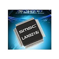
LAN9218I-MT SMSC, LAN9218I-MT Datasheet - Page 30

LAN9218I-MT
Manufacturer Part Number
LAN9218I-MT
Description
Ethernet ICs Indust Hi Perfrm Single-Chip
Manufacturer
SMSC
Type
Single Chip MAC and PHY Controllerr
Datasheet
1.LAN9218I-MT.pdf
(133 pages)
Specifications of LAN9218I-MT
Ethernet Connection Type
10 Base-T, 100 Base-TX
Minimum Operating Temperature
- 40 C
Mounting Style
SMD/SMT
Product
Ethernet Controllers
Number Of Transceivers
1
Standard Supported
802.3, 802.3u
Data Rate
10 Mbps, 100 Mbps
Supply Voltage (max)
3.3 V
Supply Voltage (min)
0 V
Supply Current (max)
69 mA
Maximum Operating Temperature
+ 85 C
Package / Case
TQFP-100
Lead Free Status / RoHS Status
Lead free / RoHS Compliant
Available stocks
Company
Part Number
Manufacturer
Quantity
Price
Company:
Part Number:
LAN9218I-MT
Manufacturer:
Standard
Quantity:
1 981
Company:
Part Number:
LAN9218I-MT
Manufacturer:
SMSC
Quantity:
6
Part Number:
LAN9218I-MT
Manufacturer:
SMSC
Quantity:
20 000
Revision 2.7 (03-15-10)
3.7
3.8
Default Mode - Word Swap Register equal to 0x00000000 or any value other than 0xFFFFFFFF
Word Swap Mode - Word Swap Register equal to 0xFFFFFFFF
ADDRESS
A1 PIN
register affects how words on the data bus are written to or read from the Control and Status Registers
and the Transmit and Receive Data/Status FIFOs. Refer to
mode only)"
FIFO to the network, the low order word is always transmitted first, and when the LAN9218i receives
data from the network to the Receive Data FIFO, the low-order word is always received first.
This register only takes effect when the LAN9218i is configured to operate in 16-bit mode. In 32-bit
mode, this register is ignored and the upper data bits, D[31:16], are always mapped to the high-order
word, and the lower data bits, D[15:0] are always mapped to the low-order word.
The General Purpose Timer is a programmable block that can be used to generate periodic host
interrupts. The resolution of this timer is 100uS.
The GP Timer loads the GPT_CNT Register with the value in the GPT_LOAD field and begins counting
down when the TIMER_EN bit is set to a ‘1.’ On a reset, or when the TIMER_EN bit changes from
set ‘1’ to cleared ‘0,’ the GPT_LOAD field is initialized to FFFFh. The GPT_CNT register is also
initialized to FFFFh on a reset. Software can write the pre-load value into the GPT_LOAD field at any
time; e.g., before or after the TIMER_EN bit is asserted. The GPT Enable bit TIMER_EN is located in
the GPT_CFG register.
Once enabled, the GPT counts down either until it reaches 0000h or until a new pre-load value is
written to the GPT_LOAD field. At 0000h, the counter wraps around to FFFFh, asserts the GPT
interrupt status bit and the IRQ signal if the GPT_INT_EN bit is set, and continues counting. The GPT
interrupt status bit is in the INT_STS Register. The GPT_INT hardware interrupt can only be set if the
GPT_INT_EN bit is set. GPT_INT is a sticky bit (R/WC); i.e., once the GPT_INT bit is set, it can only
be cleared by writing a ‘1’ to the bit.
The LAN9218i can optionally load its MAC address from an external serial EEPROM. If a properly
configured EEPROM is detected by the LAN9218i at power-up, hard reset or soft reset, the ADDRH
and ADDRL registers will be loaded with the contents of the EEPROM. If a properly configured
EEPROM is not detected, it is the responsibility of the host LAN Driver to set the IEEE addresses.
General Purpose Timer (GP Timer)
EEPROM Interface
A1 = 0
A1 = 1
A1 = 0
A1 = 1
below for more details. Whenever the LAN9218i transmits data from the Transmit Data
Table 3.7 Word Swap Control (16-bit mode only)
D[15:8]
Byte 1
Byte 3
Byte 3
Byte 1
BYTE ORDER
High-Performance Single-Chip 10/100 Ethernet Controller with HP Auto-MDIX and Industrial Temperature Support
DATASHEET
Byte 0
Byte 2
Byte 2
Byte 0
D[7:0]
30
When A1=0, D[15:0] is mapped to the low order
words of CSRs and FIFOs. When A1=1, D[15:0] is
mapped to the high-order words of CSRs and
FIFOs. Since low-order words are always
transmitted/received first, A1=0 data will always
precede A1=1 data.
When A1=0, D[15:0] is mapped to the high order
words of CSRs and FIFOs. When A1=1, D[15:0] is
mapped to the low order words of CSRs and FIFOs.
In this case A1=1 data will always precede A1=0
data.
Table 3.7, "Word Swap Control (16-bit
DESCRIPTION
SMSC LAN9218i
Datasheet


