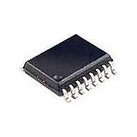
SI2400-BSR Silicon Laboratories Inc, SI2400-BSR Datasheet - Page 67

SI2400-BSR
Manufacturer Part Number
SI2400-BSR
Description
Telecom Line Management ICs CONTACT SILICON LABS FOR AVAILABILITY
Manufacturer
Silicon Laboratories Inc
Type
Integrated Global DAAr
Datasheet
1.SI2400-BS.pdf
(94 pages)
Specifications of SI2400-BSR
Product
Modem Chip
Supply Voltage (min)
3 V
Supply Current
21 mA
Maximum Operating Temperature
+ 85 C
Minimum Operating Temperature
- 40 C
Mounting Style
SMD/SMT
Package / Case
SOIC-16
Lead Free Status / RoHS Status
Lead free / RoHS Compliant
- Current page: 67 of 94
- Download datasheet (2Mb)
SE4 (CF5). Chip Functions 5
Reset settings = 0000_0000
*Note: GPE and TRSP are mutually exclusive. Only one can be set at any one time, and they override the settings in registers
Name
Type
Bit
5:4
Bit
7
6
3
2
1
0
GPIO2 and GPIO1. Once TXD2 and RXD2 are enabled through TRSP
longer function and pins TXD2 and RXD2 control the Si2400. This feature allows a second microcontroller to control
the Si2400.
NBCK
Reserved
D7
TRSP*
R
Name
NBCK
SBCK
GPE*
APO
DRT
SBCK
D6
R
9600 Baud Clock (Read Only).
600 Baud Clock (Read Only).
Data Routing (See Figure 10).
00 = Data mode, DSP output transmitted to line, line received by DSP input.
01 = Voice mode, selected AIN transmitted to line, line received by AOUT.
10 = Loopback mode, RXD through microcontroller (DSP) to TXD. AIN looped to AOUT.
11 = Codec mode, data from DSPOUT to AOUT, AIN to DSPIN.
GPIO1 Enable.
0 = Disable.
1 = Enable GPIO1 to be HDLC end-of-frame flag.
Read returns zero.
Analog Power On.
0 = Disable.
1 = Power on analog ADC and DAC.
TXD2/RXD2 Serial Port.
0 = Disable.
1 = Enable TXD2/RXD2 serial port so that RXD2 is GPIO1 and TXD2 is GPIO2.
b
(0x00)
D5
DRT
R/W
D4
GPE
R/W
D3
Rev. 1.3
D2
Function
APO
R/W
D1
=
1
b
, the primary serial port TXD and RXD no
TRSP
R/W
D0
Si2400
67
Related parts for SI2400-BSR
Image
Part Number
Description
Manufacturer
Datasheet
Request
R

Part Number:
Description:
IC ISOMODEM SYSTEM-SIDE 16SOIC
Manufacturer:
Silicon Laboratories Inc
Datasheet:

Part Number:
Description:
2400 BPS ISOMODEM EM SYSTEM-SIDE
Manufacturer:
Silicon Laboratories Inc
Datasheet:

Part Number:
Description:
IC ISOMODEM SYSTEM-SIDE 16SOIC
Manufacturer:
Silicon Laboratories Inc
Datasheet:

Part Number:
Description:
Telecom Line Management ICs 2400b/s System Side
Manufacturer:
Silicon Laboratories Inc
Datasheet:
Part Number:
Description:
SI2400 ISOMODEM LINE-SIDE
Manufacturer:
Silicon Laboratories Inc
Datasheet:
Part Number:
Description:
SMD/C°/SINGLE-ENDED OUTPUT SILICON OSCILLATOR
Manufacturer:
Silicon Laboratories Inc
Part Number:
Description:
Manufacturer:
Silicon Laboratories Inc
Datasheet:
Part Number:
Description:
N/A N/A/SI4010 AES KEYFOB DEMO WITH LCD RX
Manufacturer:
Silicon Laboratories Inc
Datasheet:
Part Number:
Description:
N/A N/A/SI4010 SIMPLIFIED KEY FOB DEMO WITH LED RX
Manufacturer:
Silicon Laboratories Inc
Datasheet:
Part Number:
Description:
N/A/-40 TO 85 OC/EZLINK MODULE; F930/4432 HIGH BAND (REV E/B1)
Manufacturer:
Silicon Laboratories Inc
Part Number:
Description:
EZLink Module; F930/4432 Low Band (rev e/B1)
Manufacturer:
Silicon Laboratories Inc
Part Number:
Description:
I°/4460 10 DBM RADIO TEST CARD 434 MHZ
Manufacturer:
Silicon Laboratories Inc
Part Number:
Description:
I°/4461 14 DBM RADIO TEST CARD 868 MHZ
Manufacturer:
Silicon Laboratories Inc


