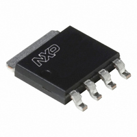
PSMN7R0-30YL,115 NXP Semiconductors, PSMN7R0-30YL,115 Datasheet - Page 3

PSMN7R0-30YL,115
Manufacturer Part Number
PSMN7R0-30YL,115
Description
MOSFET N-CH 30V 65A LFPAK
Manufacturer
NXP Semiconductors
Datasheet
1.PSMN7R0-30YL115.pdf
(14 pages)
Specifications of PSMN7R0-30YL,115
Package / Case
LFPak-4
Fet Type
MOSFET N-Channel, Metal Oxide
Fet Feature
Logic Level Gate
Rds On (max) @ Id, Vgs
7 mOhm @ 15A, 10V
Drain To Source Voltage (vdss)
30V
Current - Continuous Drain (id) @ 25° C
65A
Vgs(th) (max) @ Id
2.15V @ 1mA
Gate Charge (qg) @ Vgs
22nC @ 10V
Input Capacitance (ciss) @ Vds
1270pF @ 12V
Power - Max
51W
Mounting Type
Surface Mount
Minimum Operating Temperature
- 55 C
Configuration
Single Triple Source
Transistor Polarity
N-Channel
Resistance Drain-source Rds (on)
7 mOhms
Drain-source Breakdown Voltage
30 V
Gate-source Breakdown Voltage
20 V
Continuous Drain Current
76 A
Power Dissipation
51 W
Maximum Operating Temperature
+ 175 C
Mounting Style
SMD/SMT
Fall Time
11 ns
Rise Time
39 ns
Lead Free Status / RoHS Status
Lead free / RoHS Compliant
Lead Free Status / RoHS Status
Lead free / RoHS Compliant, Lead free / RoHS Compliant
Other names
568-4686-2
934063077115
PSMN7R0-30YL T/R
934063077115
PSMN7R0-30YL T/R
NXP Semiconductors
PSMN7R0-30YL
Product data sheet
Fig 1.
Fig 3.
(A)
(A)
I
10
I
D
10
D
10
100
10
80
60
40
20
-1
3
2
1
0
10
mounting base temperature
Continuous drain current as a function of
Safe operating area; continuous and peak drain currents as a function of drain-source voltage
0
-1
50
100
Limit R
150
DSon
All information provided in this document is subject to legal disclaimers.
T
003aac720
mb
1
= V
(°C)
DS
200
/ I
Rev. 04 — 9 March 2011
D
DC
N-channel 30 V 7 mΩ logic level MOSFET in LFPAK
Fig 2.
P
(%)
der
120
80
40
0
function of mounting base temperature
Normalized total power dissipation as a
0
10
50
PSMN7R0-30YL
100
V
DS
10 μs
100 μs
1 ms
10 ms
100 ms
(V)
150
© NXP B.V. 2011. All rights reserved.
T
003aac732
mb
03aa16
(°C)
10
200
2
3 of 14


