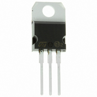
STP40NF10L STMicroelectronics, STP40NF10L Datasheet - Page 8

STP40NF10L
Manufacturer Part Number
STP40NF10L
Description
MOSFET N-CH 100V 40A TO-220
Manufacturer
STMicroelectronics
Series
STripFET™r
Datasheet
1.STP40NF10L.pdf
(12 pages)
Specifications of STP40NF10L
Fet Type
MOSFET N-Channel, Metal Oxide
Fet Feature
Logic Level Gate
Rds On (max) @ Id, Vgs
33 mOhm @ 20A, 10V
Drain To Source Voltage (vdss)
100V
Current - Continuous Drain (id) @ 25° C
40A
Vgs(th) (max) @ Id
2.5V @ 250µA
Gate Charge (qg) @ Vgs
64nC @ 5V
Input Capacitance (ciss) @ Vds
2300pF @ 25V
Power - Max
150W
Mounting Type
Through Hole
Package / Case
TO-220-3 (Straight Leads)
Configuration
Single
Transistor Polarity
N-Channel
Resistance Drain-source Rds (on)
0.033 Ohms
Forward Transconductance Gfs (max / Min)
25 S
Drain-source Breakdown Voltage
100 V
Gate-source Breakdown Voltage
+/- 17 V
Continuous Drain Current
40 A
Power Dissipation
150 W
Maximum Operating Temperature
+ 175 C
Mounting Style
Through Hole
Minimum Operating Temperature
- 65 C
Lead Free Status / RoHS Status
Lead free / RoHS Compliant
Other names
497-6741-5
STP40NF10L
STP40NF10L
Available stocks
Company
Part Number
Manufacturer
Quantity
Price
Company:
Part Number:
STP40NF10L
Manufacturer:
ST
Quantity:
12 500
3
Figure 13. Switching times test circuit for
Figure 15. Test circuit for inductive load
Figure 17. Unclamped inductive waveform
Test circuit
8/12
resistive load
switching and diode recovery times
Test circuit
Figure 14. Gate charge test circuit
Figure 16. Unclamped Inductive load test
Figure 18. Switching time waveform
circuit
STP40NF10L


