STP200N6F3 STMicroelectronics, STP200N6F3 Datasheet
STP200N6F3
Specifications of STP200N6F3
Available stocks


Related parts for STP200N6F3


STP200N6F3 Summary of contents
Page 1
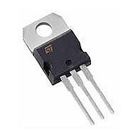
... STripFET™ Power MOSFET (1) 120 A 330 W (1) 120 A 330 W (1) 120 A 330 W TO-220 Figure 1. Marking Package 200N6F3 D 2 200N6F3 I 200N6F3 TO-220 Doc ID 15606 Rev 2 STP200N6F3 2 PAK, TO-220 PAK I PAK Internal schematic diagram Packaging 2 PAK Tape and reel PAK Tube Tube 2 PAK 3 ...
Page 2
... Contents Contents 1 Electrical ratings . . . . . . . . . . . . . . . . . . . . . . . . . . . . . . . . . . . . . . . . . . . . 3 2 Electrical characteristics . . . . . . . . . . . . . . . . . . . . . . . . . . . . . . . . . . . . . 4 2.1 Electrical characteristics (curves) 3 Test circuits 4 Package mechanical data . . . . . . . . . . . . . . . . . . . . . . . . . . . . . . . . . . . . 10 5 Packaging mechanical data . . . . . . . . . . . . . . . . . . . . . . . . . . . . . . . . . . 14 6 Revision history . . . . . . . . . . . . . . . . . . . . . . . . . . . . . . . . . . . . . . . . . . . 15 2/16 STB200N6F3, STI200N6F3, STP200N6F3 . . . . . . . . . . . . . . . . . . . . . . . . . . . . . . . . . . . . . . . . . . . . . . 9 Doc ID 15606 Rev ...
Page 3
... STB200N6F3, STI200N6F3, STP200N6F3 1 Electrical ratings Table 2. Absolute maximum ratings Symbol V Drain-source voltage ( Gate-source voltage GS (1) I Drain current (continuous (1) I Drain current (continuous (2) I Drain current (pulsed Total dissipation at T TOT Derating factor (3) E Single pulse avalanche energy AS T Operating junction temperature ...
Page 4
... D²PAK TO-220, I²PAK Parameter Test conditions 1MHz 4.7 Ω (see Figure 15, Figure 20 Figure 16) (see Doc ID 15606 Rev 2 STB200N6F3, STI200N6F3, STP200N6F3 Min. Typ. Max ± = 250 µ 3.3 Min. Typ. Max. 6265 - 1295 120 A, 101 25.2 Unit V 10 µA 100 µA ...
Page 5
... STB200N6F3, STI200N6F3, STP200N6F3 Table 6. Source drain diode Symbol Source-drain current I SD Source-drain current (1) I SDM (pulsed) (2) V Forward on voltage SD t Reverse recovery time rr Q Reverse recovery charge rr I Reverse recovery current RRM 1. Pulse width limited by safe operating area 2. Pulsed: pulse duration = 300µs, duty cycle 1.5% ...
Page 6
... DS Figure Figure 7. AM05516v1 350 300 250 200 6V 150 100 (V) DS Doc ID 15606 Rev 2 STB200N6F3, STI200N6F3, STP200N6F3 Thermal impedance for TO-220, I²PAK δ=0.5 0.2 0.1 0.05 0.02 Zth=k Rthj-c δ=tp/τ 0.01 Single pulse tp τ Thermal impedance for D²PAK δ=0.5 ...
Page 7
... STB200N6F3, STI200N6F3, STP200N6F3 Figure 8. Normalized B VDSS BV DSS (norm) 1.06 1.03 1.00 0.98 0.95 0.92 -50 - Figure 10. Gate charge vs gate-source voltage Figure 11. Capacitance variations V GS (V) V =30V =120A Figure 12. Normalized gate threshold voltage vs temperature vs temperature Figure 9. AM00897v1 R DS(on) (mΩ (°C) 100 J AM05520v1 14010 ...
Page 8
... Electrical characteristics Figure 14. Source-drain diode forward characteristics V SD (V) 0.9 T =-55°C J 0.8 0.7 0.6 0.5 0.4 0 8/16 AM05524v1 T =25° =175° ( Doc ID 15606 Rev 2 STB200N6F3, STI200N6F3, STP200N6F3 ...
Page 9
... STB200N6F3, STI200N6F3, STP200N6F3 3 Test circuits Figure 15. Switching times test circuit for resistive load D.U. Figure 17. Test circuit for inductive load switching and diode recovery times FAST L=100µH G D.U.T. DIODE Ω Figure 19. Unclamped inductive waveform Figure 16. Gate charge test circuit 3.3 2200 µ ...
Page 10
... Package mechanical data 4 Package mechanical data In order to meet environmental requirements, ST offers these devices in different grades of ® ECOPACK packages, depending on their level of environmental compliance. ECOPACK specifications, grade definitions and product status are available at: www.st.com. ECOPACK trademark. 10/16 STB200N6F3, STI200N6F3, STP200N6F3 Doc ID 15606 Rev 2 ® ...
Page 11
... STB200N6F3, STI200N6F3, STP200N6F3 Dim D2PAK (TO-263) mechanical data m m Min Typ Max ° 0 ° 8 0079457_M Doc ID 15606 Rev 2 Package mechanical data Min Typ Max ° 0 ° 8 11/16 ...
Page 12
... Package mechanical data Dim 12/16 STB200N6F3, STI200N6F3, STP200N6F3 I²PAK (TO-262) mechanical data mm Min Typ Max 4.40 4.60 2.40 2.72 0.61 0.88 1.14 1.70 0.49 0.70 1.23 1.32 8.95 9.35 2.40 2.70 4.95 5.15 10 10. 3.50 3.93 1.27 1.40 Doc ID 15606 Rev 2 ...
Page 13
... STB200N6F3, STI200N6F3, STP200N6F3 TO-220 type A mechanical data Dim Min A 4.40 b 0.61 b1 1.14 c 0.48 D 15. 2.40 e1 4.95 F 1.23 H1 6. 3.50 L20 L30 ∅P 3.75 Q 2.65 Doc ID 15606 Rev 2 Package mechanical data mm Typ Max 4.60 0.88 1.70 0.70 15.75 1.27 10.40 2.70 5 ...
Page 14
... Doc ID 15606 Rev 2 STB200N6F3, STI200N6F3, STP200N6F3 REEL MECHANICAL DATA mm DIM. MIN. MAX. MIN. A 330 B 1.5 0.059 C 12.8 13.2 ...
Page 15
... STB200N6F3, STI200N6F3, STP200N6F3 6 Revision history Table 7. Document revision history Date 20-Apr-2009 18-Nov-2009 Revision 1 First version. 2 Document status promoted from preliminary data to datasheet. Doc ID 15606 Rev 2 Revision history Changes 15/16 ...
Page 16
... Australia - Belgium - Brazil - Canada - China - Czech Republic - Finland - France - Germany - Hong Kong - India - Israel - Italy - Japan - Malaysia - Malta - Morocco - Philippines - Singapore - Spain - Sweden - Switzerland - United Kingdom - United States of America 16/16 STB200N6F3, STI200N6F3, STP200N6F3 Please Read Carefully: © 2009 STMicroelectronics - All rights reserved STMicroelectronics group of companies www ...