TK15J60U(F) Toshiba, TK15J60U(F) Datasheet
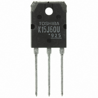
MOSFET N-CH 600V 15A TO-3P

TK15J60U(F)

Manufacturer Part Number
TK15J60U(F)
Description
MOSFET N-CH 600V 15A TO-3P
Manufacturer
Toshiba
Datasheet

Specifications of TK15J60U(F)

Fet Type
MOSFET N-Channel, Metal Oxide
Fet Feature
Standard
Rds On (max) @ Id, Vgs
300 mOhm @ 7.5A, 10V
Drain To Source Voltage (vdss)
600V
Current - Continuous Drain (id) @ 25° C
15A
Vgs(th) (max) @ Id
5V @ 1mA
Gate Charge (qg) @ Vgs
17nC @ 10V
Input Capacitance (ciss) @ Vds
950pF @ 10V
Power - Max
170W
Mounting Type
Through Hole
Package / Case
TO-3P
Configuration
Single
Transistor Polarity
N-Channel
Resistance Drain-source Rds (on)
0.3 Ohms
Drain-source Breakdown Voltage
600 V
Gate-source Breakdown Voltage
+/- 30 V
Continuous Drain Current
15 A
Power Dissipation
170 W
Maximum Operating Temperature
+ 150 C
Mounting Style
Through Hole
Minimum Operating Temperature
- 55 C
Lead Free Status / RoHS Status
Lead free / RoHS Compliant
Other names
TK15J60U(F)

Available stocks

Company
Part Number
Manufacturer
Quantity
Price
Part Number:
TK15J60U(F)
Manufacturer:
TOS
Quantity:
2 522
Switching Regulator Applications
Absolute Maximum Ratings
Thermal Characteristics
This transistor is an electrostatic sensitive device. Please handle with caution.
Low drain-source ON resistance: R
High forward transfer admittance: ⎪Y
Low leakage current: I
Enhancement-mode: V
Drain-source voltage
Gate-source voltage
Drain current
Drain power dissipation (Tc = 25°C)
Single pulse avalanche energy
Avalanche current
Repetitive avalanche energy
Channel temperature
Storage temperature range
Note:
Thermal resistance, channel to case
Thermal resistance, channel to ambient
Note 1: Please use devices on conditions that the channel temperature is below 150°C.
Note 2: V
Note 3: Repetitive rating: pulse width limited by maximum channel temperature
Using continuously under heavy loads (e.g. the application of high temperature/current/voltage and the
significant change in temperature, etc.) may cause this product to decrease in the reliability significantly
even if the operating conditions (i.e. operating temperature/current/voltage, etc.) are within the absolute
maximum ratings. Please design the appropriate reliability upon reviewing the Toshiba Semiconductor
Reliability Handbook (“Handling Precautions”/“Derating Concept and Methods”) and individual reliability
data (i.e. reliability test report and estimated failure rate, etc).
Characteristics
DD
TOSHIBA Field Effect Transistor Silicon N Channel MOS Type (DTMOSⅡ)
Characteristics
= 90 V, T
DC
Pulse (t = 1 ms)
DSS
ch
th
= 25°C (initial), L = 0.63 mH, R
= 3.0~5.0 V (V
(Note 1)
(Note 1)
(Note 2)
(Note 3)
= 100 μA (V
DS (ON)
(Ta = 25°C)
Symbol
V
V
fs
TK15J60U
E
E
T
I
I
T
GSS
P
DSS
I
DP
AR
⎪ = 8.5 S (typ.)
DS
AS
AR
stg
D
ch
R
R
D
DS
Symbol
th (ch-a)
th (ch-c)
= 10 V, I
= 0.24Ω (typ.)
= 600 V)
−55 to 150
D
Rating
600
±30
170
150
15
30
81
15
17
= 1 mA)
1
0.735
G
Max
50
= 25Ω, I
Unit
AR
mJ
mJ
°C/W
°C/W
°C
°C
W
V
V
A
A
Unit
= 15 A
Weight : 4.6 g (typ.)
JEDEC
JEITA
TOSHIBA
1.0
5.45 ± 0.2
2.0 ± 0.3
+0.3
−0.25
1. Gate
2. Drain(heat sink)
3. Source
1
15.9 MAX.
2
1
3
5.45 ± 0.2
2-16C1B
SC-65
TK15J60U
Ф3.2 ± 0.2
2008-06-11
Unit: mm
2
3

Related parts for TK15J60U(F)

TK15J60U(F) Summary of contents

Page 1

... Please design the appropriate reliability upon reviewing the Toshiba Semiconductor Reliability Handbook (“Handling Precautions”/“Derating Concept and Methods”) and individual reliability data (i ...

Page 2

... Source-Drain Ratings and Characteristics Characteristics Continuous drain reverse current (Note 1) Pulse drain reverse current (Note 1) Forward voltage (diode) Reverse recovery time Reverse recovery charge Marking TOSHIBA K15J60U Part No. (or abbreviation code) Lot No. A line indicates Lead (Pb)-Free (Ta = 25°C) Symbol Test Condition = ± ...

Page 3

I – Common source Tc = 25° Pulse test 5 Drain−source voltage V ( – V ...

Page 4

R – (ON) 1 Common source Pulse test 0.8 7.5 0 0.4 0.2 0 −80 − 120 Case temperature Tc (°C) C – V ...

Page 5

Duty=0.5 0.2 0.1 0.05 0.1 Single pulse 0.01 0.02 0.01 10μ 100μ Safe operating area 100 100 µ max (Pulse max (Continuous operation Tc = 25°C 1 0.1 * Single ...

Page 6

... The information contained herein is presented only as a guide for the applications of our products. No responsibility is assumed by TOSHIBA for any infringements of patents or other rights of the third parties which may result from its use. No license is granted by implication or otherwise under any patents or other rights of TOSHIBA or the third parties. • ...

Related keywords