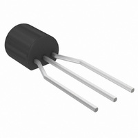
BS170G ON Semiconductor, BS170G Datasheet - Page 3

BS170G
Manufacturer Part Number
BS170G
Description
MOSFET N-CH 60V 500MA TO-92
Manufacturer
ON Semiconductor
Type
Small Signalr
Specifications of BS170G
Fet Type
MOSFET N-Channel, Metal Oxide
Fet Feature
Standard
Rds On (max) @ Id, Vgs
5 Ohm @ 200mA, 10V
Drain To Source Voltage (vdss)
60V
Current - Continuous Drain (id) @ 25° C
500mA
Vgs(th) (max) @ Id
3V @ 1mA
Input Capacitance (ciss) @ Vds
60pF @ 10V
Power - Max
350mW
Mounting Type
Through Hole
Package / Case
TO-92-3 (Standard Body), TO-226
Configuration
Single
Transistor Polarity
N-Channel
Resistance Drain-source Rds (on)
5 Ohm @ 10 V
Forward Transconductance Gfs (max / Min)
0.2 S
Drain-source Breakdown Voltage
60 V
Gate-source Breakdown Voltage
+/- 20 V
Continuous Drain Current
0.5 A
Power Dissipation
350 mW
Maximum Operating Temperature
+ 150 C
Mounting Style
Through Hole
Minimum Operating Temperature
- 55 C
Current, Drain
0.5 A
Package Type
TO-92 (TO-226)
Polarization
N-Channel
Resistance, Drain To Source On
1.8 Ohms
Temperature, Operating, Maximum
+150 °C
Temperature, Operating, Minimum
-55 °C
Transconductance, Forward
200 Millimhos
Voltage, Breakdown, Drain To Source
90 V
Voltage, Gate To Source
±20 VDC
Number Of Elements
1
Polarity
N
Channel Mode
Enhancement
Drain-source On-res
5Ohm
Drain-source On-volt
60V
Gate-source Voltage (max)
±20V
Operating Temp Range
-55C to 150C
Operating Temperature Classification
Military
Mounting
Through Hole
Pin Count
3
Lead Free Status / RoHS Status
Lead free / RoHS Compliant
Gate Charge (qg) @ Vgs
-
Lead Free Status / Rohs Status
Lead free / RoHS Compliant
Other names
BS170G
BS170GOS
BS170GOS
Available stocks
Company
Part Number
Manufacturer
Quantity
Price
Company:
Part Number:
BS170G
Manufacturer:
ON Semiconductor
Quantity:
4 450
Part Number:
BS170G
Manufacturer:
ON/安森美
Quantity:
20 000
Part Number:
BS170G.
Manufacturer:
ON/安森美
Quantity:
20 000
PULSE GENERATOR
2.0
1.6
1.2
0.8
0.4
0.8
2.0
1.6
1.2
0.4
0
50 W
50
0
Figure 3. V
Figure 1. Switching Test Circuit
V
Figure 5. Output Characteristics
DS
, DRAIN−TO−SOURCE VOLTAGE (VOLTS)
GS(th)
10
V
T
0
in
J
50 W
, JUNCTION TEMPERATURE (°C)
Normalized versus Temperature
40 pF
20
50
1.0 MW
V
I
+25 V
D
DS
= 1.0 mA
125 W
100
30
= V
(V
GS
50 W ATTENUATOR
in
V
RESISTIVE SWITCHING
GS
Amplitude 10 Volts)
= 10 V
http://onsemi.com
9.0 V
8.0 V
7.0 V
5.0 V
6.0 V
4.0 V
20 dB
40
150
BS170
3
100
TO SAMPLING SCOPE
50 W INPUT
80
60
40
20
2.0
1.6
1.2
0.8
0.4
0
0
V
out
10
Figure 4. On−Region Characteristics
V
OUTPUT
INVERTED
V
DS
INPUT
Figure 6. Capacitance versus
DS
, DRAIN−TO−SOURCE VOLTAGE (VOLTS)
Drain−To−Source Voltage
Figure 2. Switching Waveforms
, DRAIN−TO−SOURCE VOLTAGE (VOLTS)
1.0
20
V
GS
V
V
in
= 0 V
out
10%
30
2.0
t
on
40
90%
PULSE
WIDTH
50
3.0
V
60
GS
C
t
90%
C
C
off
oss
= 10 V
iss
rss
50%
9.0 V
8.0 V
7.0 V
6.0 V
5.0 V
4.0 V
10%
4.0


