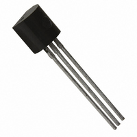
ZVN3320ASTOA Diodes Zetex, ZVN3320ASTOA Datasheet - Page 34

ZVN3320ASTOA
Manufacturer Part Number
ZVN3320ASTOA
Description
MOSFET N-CHAN 200V TO92-3
Manufacturer
Diodes Zetex
Datasheet
1.BAT1000TA.pdf
(96 pages)
Specifications of ZVN3320ASTOA
Fet Type
MOSFET N-Channel, Metal Oxide
Fet Feature
Standard
Rds On (max) @ Id, Vgs
25 Ohm @ 100mA, 10V
Drain To Source Voltage (vdss)
200V
Current - Continuous Drain (id) @ 25° C
100mA
Vgs(th) (max) @ Id
3V @ 1mA
Input Capacitance (ciss) @ Vds
45pF @ 25V
Power - Max
625mW
Mounting Type
Through Hole
Package / Case
TO-92-3 (Standard Body), TO-226
Lead Free Status / RoHS Status
Lead free / RoHS Compliant
Gate Charge (qg) @ Vgs
-
Other names
ZVN3320ASTOA
ZVN3320ASTOATR
ZVN3320ASTOATR
Article
Applications dictate bipolar or MOSFET power switch choices
Bipolar transistors have continued
to be developed to rival or exceed
MOSFET performance in many
applications. It’s therefore important
to review the characteristics and
benefits of each technology to
extract the best system performance.
The first characteristic that designers
often consider is on-state resistance
for a given breakdown voltage. Figure
1 shows the rapid advances made by
Zetex in recent years. Furthermore,
bipolar transistors benefit from
conductivity modulation, an effect that
increases the advantage that the
bipolar transistors hold over MOSFETs
as breakdown voltages increase.
Also, don’t forget that bipolar
transistors block voltage in two
directions, as specified by their BV
or BV
eliminate the need for a series diode
and its attendant conduction losses.
(See Application example 1.)
How resistance changes with
temperature affects the current
capability of a power switch. The rise
in bipolar R
of a MOSFET’s equivalent R
leading to cooler running and higher
continuous currents.
Drive requirements are arguably
where bipolars and MOSFETs differ
most and care must be taken to
account for the bipolar’s base drive
loss in power dissipation calculations.
However, bipolars are fully turned on
at around one volt, whereas the
achievable R
be limited in low voltage applications
by the available drive voltage over
threshold.
Figure 1. Specific on-resistance (20V devices)
150
130
110
90
70
50
30
10
ECO
Section 1.1
characteristic which can
CE(sat)
DS(on)
is generally half that
of a MOSFET may
Year
DS(on)
EBO
Figure 2. A typical linear
charger circuit
Bipolars are slower switching than
MOSFETs when operated as a
saturated switch, provided the
MOSFET has a sufficiently high-
current drive. Ironically perhaps,
bipolars are often employed as
MOSFET pre-drivers, exploiting their
high-current capabilities and fast
switching speed when operating in
the linear region (see Application
example 2).
By understanding the relative strengths
and weaknesses of each technology
the performance-cost relationship can
be maximized. A summary of the key
parametric differences of the
competing technologies appears in the
table opposite.
Application example 1:
Linear mode battery charging
Linear chargers are simple, small, and
emit no EMI making them suitable for
low noise environments. They use an
external pass element to drop the
voltage from the input supply to the
battery voltage thus power dissipation
is high. A typical linear charger circuit
is shown in Figure 2.
NPN
PNP
AC Line
Adapter
34
C
Figure 3. Totem-pole driver stage for power MOSFET
IN
R
C
COMP
COMP
V
CFLG
COMP/DIS
CC
OUT
GND
Power losses in the transistor are
dominated by the collector-emitter
losses:
P
where V
and the selection criteria usually
include current capability, gain, cost,
and package dissipation. Bipolar PNP
transistors are advantageous in this
application because of their bi-
directional blocking capability, whereas
a MOSFET requires a series Schottky
diode to prevent current flowing from
the battery to the supply, through its
body diode.
Application example 2:
MOSFET gate drivers
High current low R
exhibit gate capacitances that require
amps of drive current. For example,
a typical 100V MOSFET with a gate
charge of 50nC, requires 2.5 amps to
switch in 20ns.
Bipolar transistors are ideally suited as
gate drivers because they feature fast
switching in linear mode, high pulse-
current capability, and high current
density - hence small size and cost.
One of the most popular and cost-
effective drive circuits is a bipolar,
non-inverting totem-pole driver
(see Figure 3)
D(CE)
T
SENSE
V
I
SNS
SNS
= I
R
THM
CHG
SENSE
V
x (V
DRIVE
R
= I
Q1
Q2
SENSE
IN
C
CHG
R
OUT
- V
DS(on)
GATE
DCD
x R
Li-Ion
cell
MOSFETs can
SENSE
- V
SENSE
V
(V)
CC
) (W)
RL


