NDB6020P Fairchild Semiconductor, NDB6020P Datasheet
NDB6020P
Specifications of NDB6020P
NDB6020PTR
Available stocks


Related parts for NDB6020P


NDB6020P Summary of contents
Page 1
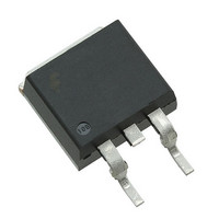
... NDP6020P / NDB6020P P-Channel Logic Level Enhancement Mode Field Effect Transistor General Description These logic level P-Channel enhancement mode power field effect transistors are produced using Fairchild's proprietary, high cell density, DMOS technology. This very high density process has been especially tailored to minimize on-state ...
Page 2
Electrical Characteristics (T = 25°C unless otherwise noted) C Symbol Parameter OFF CHARACTERISTICS BV Drain-Source Breakdown Voltage DSS I Zero Gate Voltage Drain Current DSS I Gate - Body Leakage, Forward GSSF I Gate - Body Leakage, Reverse GSSR ON ...
Page 3
Electrical Characteristics (T = 25°C unless otherwise noted) C Symbol Parameter DRAIN-SOURCE DIODE CHARACTERISTICS I Maximum Continuous Drain-Source Diode Forward Current S Maximum Pulsed Drain-Source Diode Forward Current Drain-Source Diode Forward Voltage SD Reverse Recovery Time t ...
Page 4
Typical Electrical Characteristics - -5.0V GS -4.5 -4.0 -40 -3.5 -30 -20 - DRAIN-SOURCE VOLTAGE (V) DS Figure 1. On-Region Characteristics. 1 -12A D 1.6 V =-4. ...
Page 5
Typical Electrical Characteristics -250µ ...
Page 6
Typical Electrical Characteristics -10 - DRAIN CURRENT (A) D Figure 13. Transconductance Variation with Drain . Current and Temperature 0.5 0.5 0.3 ...