IRF6617 International Rectifier, IRF6617 Datasheet - Page 2
IRF6617
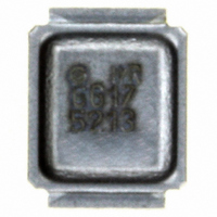
Manufacturer Part Number
IRF6617
Description
MOSFET N-CH 30V 14A DIRECTFET
Manufacturer
International Rectifier
Series
HEXFET®r
Datasheet
1.IRF6617.pdf
(9 pages)
Specifications of IRF6617
Fet Type
MOSFET N-Channel, Metal Oxide
Fet Feature
Logic Level Gate
Rds On (max) @ Id, Vgs
8.1 mOhm @ 15A, 10V
Drain To Source Voltage (vdss)
30V
Current - Continuous Drain (id) @ 25° C
14A
Vgs(th) (max) @ Id
2.35V @ 250µA
Gate Charge (qg) @ Vgs
17nC @ 4.5V
Input Capacitance (ciss) @ Vds
1300pF @ 15V
Power - Max
2.1W
Mounting Type
Surface Mount
Package / Case
DirectFET™ Isometric ST
Lead Free Status / RoHS Status
Contains lead / RoHS non-compliant
Other names
IRF6617
IRF6617TR
IRF6617TR
Available stocks
Company
Part Number
Manufacturer
Quantity
Price

Part Number:
IRF6617
Manufacturer:
IR
Quantity:
20 000
Part Number:
IRF6617TR
Manufacturer:
IR
Quantity:
20 000
Company:
Part Number:
IRF6617TR1
Manufacturer:
IOR
Quantity:
240
Company:
Part Number:
IRF6617TR1
Manufacturer:
IR
Quantity:
4 798
Part Number:
IRF6617TR1
Manufacturer:
IR
Quantity:
20 000


‚
ƒ
„
Notes:
∆ΒV
∆V
Static @ T
BV
R
V
I
I
gfs
Q
Q
Q
t
t
t
t
C
C
C
Diode Characteristics
I
I
V
t
Q
DSS
GSS
d(on)
r
d(off)
f
S
SM
rr
GS(th)
SD
DS(on)
g
Q
Q
Q
Q
sw
oss
iss
oss
rss
rr
max. junction temperature.
2
Repetitive rating; pulse width limited by
Starting T
Pulse width ≤ 400µs; duty cycle ≤ 2%.
Surface mounted on 1 in. square Cu board.
R
GS(th)
DSS
gs1
gs2
gd
godr
G
DSS
= 25Ω, I
/∆T
/∆T
J
J
J
= 25°C, L = 0.40mH,
AS
J
= 25°C (unless otherwise specified)
= 12A.
Drain-to-Source Breakdown Voltage
Breakdown Voltage Temp. Coefficient
Static Drain-to-Source On-Resistance
Gate Threshold Voltage
Gate Threshold Voltage Coefficient
Drain-to-Source Leakage Current
Gate-to-Source Forward Leakage
Gate-to-Source Reverse Leakage
Forward Transconductance
Total Gate Charge
Pre-Vth Gate-to-Source Charge
Post-Vth Gate-to-Source Charge
Gate-to-Drain Charge
Gate Charge Overdrive
Switch Charge (Q
Output Charge
Turn-On Delay Time
Rise Time
Turn-Off Delay Time
Fall Time
Input Capacitance
Output Capacitance
Reverse Transfer Capacitance
Continuous Source Current
(Body Diode)
Pulsed Source Current
(Body Diode) c
Diode Forward Voltage
Reverse Recovery Time
Reverse Recovery Charge
Parameter
Parameter
gs2
+ Q
gd
)
…
†
‡
ˆ
Used double sided cooling, mounting pad.
Mounted on minimum footprint full size board with metalized
T
R
back and with small clip heatsink.
C
θ
is measured at
measured with thermal couple mounted to top (Drain) of part.
Min. Typ. Max. Units
Min. Typ. Max. Units
1.35
–––
–––
–––
–––
–––
–––
–––
–––
–––
–––
–––
–––
–––
–––
–––
–––
–––
–––
–––
–––
–––
–––
–––
–––
–––
–––
–––
39
30
1300
0.81
–––
-5.4
–––
–––
–––
430
160
–––
–––
–––
–––
–––
6.2
7.9
3.1
1.0
4.0
2.9
5.0
3.7
7.2
25
11
10
11
34
12
16
J
-100
10.3
2.35
–––
–––
–––
150
100
–––
–––
–––
–––
–––
–––
–––
–––
–––
–––
–––
–––
–––
–––
120
1.0
1.0
8.1
17
53
24
11
mV/°C
mV/°C
mΩ
nC
nC
µA
nA
nC
pF
ns
ns
V
V
V
S
A
V
Reference to 25°C, I
V
V
V
V
V
V
V
V
V
V
I
See Fig. 16
V
V
I
Clamped Inductive Load
V
V
ƒ = 1.0MHz
MOSFET symbol
showing the
integral reverse
p-n junction diode.
T
T
di/dt = 100A/µs e
D
D
J
J
GS
GS
GS
DS
DS
DS
GS
GS
DS
DS
GS
DS
DD
GS
DS
= 12A
= 12A
= 25°C, I
= 25°C, I
= V
= 24V, V
= 24V, V
= 15V, I
= 15V
= 15V, V
= 15V
= 0V, I
= 10V, I
= 4.5V, I
= 20V
= -20V
= 4.5V
= 16V, V
= 0V
GS
, I
D
Conditions
Conditions
D
S
F
D
D
= 250µA
D
GS
GS
GS
GS
= 12A
= 12A, V
= 250µA
= 12A
= 15A e
= 12A e
= 0V
= 0V, T
= 0V
= 4.5V e
D
GS
www.irf.com
= 1mA
J
= 125°C
= 0V e
G
D
S
Related parts for IRF6617
Image
Part Number
Description
Manufacturer
Datasheet
Request
R

Part Number:
Description:
SCHOTTKY RECTIFIER
Manufacturer:
International Rectifier Corp.
Datasheet:
Part Number:
Description:
SCHOTTKY RECTIFIER
Manufacturer:
International Rectifier Corp.
Datasheet:
Part Number:
Description:
SCHOTTKY RECTIFIER
Manufacturer:
International Rectifier Corp.
Datasheet:
Part Number:
Description:
SCHOTTKY RECTIFIER
Manufacturer:
International Rectifier Corp.
Datasheet:
Part Number:
Description:
SCHOTTKY RECTIFIER
Manufacturer:
International Rectifier Corp.
Datasheet:
Part Number:
Description:
SCHOTTKY RECTIFIER
Manufacturer:
International Rectifier Corp.
Datasheet:
Part Number:
Description:
SCHOTTKY RECTIFIER
Manufacturer:
International Rectifier Corp.
Datasheet:
Part Number:
Description:
SCHOTTKY RECTIFIER
Manufacturer:
International Rectifier Corp.
Datasheet:
Part Number:
Description:
SCHOTTKY RECTIFIER
Manufacturer:
International Rectifier Corp.
Datasheet:
Part Number:
Description:
SCHOTTKY RECTIFIER
Manufacturer:
International Rectifier Corp.
Datasheet:
Part Number:
Description:
SCHOTTKY RECTIFIER
Manufacturer:
International Rectifier Corp.
Datasheet:
Part Number:
Description:
SCHOTTKY RECTIFIER
Manufacturer:
International Rectifier Corp.
Datasheet:
Part Number:
Description:
SCHOTTKY RECTIFIER
Manufacturer:
International Rectifier Corp.
Datasheet:
Part Number:
Description:
SCHOTTKY RECTIFIER
Manufacturer:
International Rectifier Corp.
Datasheet:
Part Number:
Description:
SCHOTTKY RECTIFIER
Manufacturer:
International Rectifier Corp.
Datasheet: