STW10NK80Z STMicroelectronics, STW10NK80Z Datasheet
STW10NK80Z
Specifications of STW10NK80Z
Available stocks


Related parts for STW10NK80Z


STW10NK80Z Summary of contents
Page 1
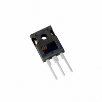
... Applications ■ Switching application Order codes Part number STP10NK80Z STP10NK80ZFP STW10NK80Z July 2006 STP10NK80Z - STW10NK80Z Zener-protected superMESH 160 W 9A 160 w TO-220 Internal schematic diagram ...
Page 2
... Electrical characteristics . . . . . . . . . . . . . . . . . . . . . . . . . . . . . . . . . . . . . 4 2.1 Electrical characteristics (curves) 3 Test circuit 4 Package mechanical data . . . . . . . . . . . . . . . . . . . . . . . . . . . . . . . . . . . . 10 5 Revision history . . . . . . . . . . . . . . . . . . . . . . . . . . . . . . . . . . . . . . . . . . . 14 2/15 STP10NK80ZFP - STP10NK80Z - STW10NK80Z . . . . . . . . . . . . . . . . . . . . . . . . . . . . . . . . . . . . . . . . . . . . . . . . ...
Page 3
... STP10NK80ZFP - STP10NK80Z - STW10NK80Z 1 Electrical ratings Table 1. Absolute maximum ratings Symbol V Drain-source voltage ( Drain-gate voltage (R DGR V Gate-source voltage GS I Drain current (continuous Drain current (continuous (2) I Drain current (pulsed Total dissipation at T TOT Derating Factor Vesd(G-S) G-S ESD (HBM C=100pF, R=1.5kΩ) ...
Page 4
... Q Gate-source charge gs Gate-drain charge Pulsed: pulse duration=300µs, duty cycle 1. defined as a constant equivalent capacitance giving the same charging time as C oss eq. inceases from 0 to 80% V 4/15 STP10NK80ZFP - STP10NK80Z - STW10NK80Z Parameter Test condictions I = 1mA Max rating Max rating @125°C GS ...
Page 5
... STP10NK80ZFP - STP10NK80Z - STW10NK80Z Table 6. Switching times Symbol t Turn-on Delay Time d(on) t Rise Time r t Turn-off Delay Time d(off) t Fall Time f Table 7. Gate-source zener diode Symbol (1) Gate-Source Breakdown BV GSO Voltage 1. The built-in back-to-back Zener diodes have specifically been designed to enhance not only the device’s ESD capability, but also to make them safely absorb possible voltage transients that may occasionally be applied from gate to source ...
Page 6
... Electrical characteristics (curves) Figure 1. Safe operating area for TO-220 Figure 3. Safe operating area for TO-220FP Figure 5. Safe operating area for TO-247 6/15 STP10NK80ZFP - STP10NK80Z - STW10NK80Z Figure 2. Thermal impedance for TO-220 Figure 4. Thermal impedance for TO-220FP Figure 6. Thermal impedance for TO-247 ...
Page 7
... STP10NK80ZFP - STP10NK80Z - STW10NK80Z Figure 7. Output characterisics Figure 9. Transconductance Figure 11. Gate charge vs gate-source voltage Figure 12. Capacitance variations Electrical characteristics Figure 8. Transfer characteristics Figure 10. Static drain-source on resistance 7/15 ...
Page 8
... Electrical characteristics Figure 13. Normalized gate threshold voltage vs temperature Figure 15. Source-drain diode forward characteristics Figure 17. Maximum avalanche energy vs temperature 8/15 STP10NK80ZFP - STP10NK80Z - STW10NK80Z Figure 14. Normalized on resistance vs temperature Figure 16. Normalized B VDSS vs temperature ...
Page 9
... STP10NK80ZFP - STP10NK80Z - STW10NK80Z 3 Test circuit Figure 18. Switching times test circuit for resistive load Figure 20. Test circuit for inductive load switching and diode recovery times Figure 22. Unclamped inductive waveform Figure 19. Gate charge test circuit Figure 21. Unclamped Inductive load test circuit Figure 23. Switching time waveform ...
Page 10
... These packages have a Lead-free second level interconnect . The category of second level interconnect is marked on the package and on the inner box label, in compliance with JEDEC Standard JESD97. The maximum ratings related to soldering conditions are also marked on the inner box label. ECOPACK trademark. ECOPACK specifications are available at: 10/15 STP10NK80ZFP - STP10NK80Z - STW10NK80Z www.st.com ...
Page 11
... STP10NK80ZFP - STP10NK80Z - STW10NK80Z DIM L20 L30 øP Q TO-220 MECHANICAL DATA mm. MIN. TYP MAX. 4.40 4.60 0.61 0.88 1.15 1.70 0.49 0.70 15.25 15.75 10 10.40 2.40 2.70 4.95 5.15 1.23 1.32 6.20 6.60 2.40 2. 3.50 3.93 16.40 28.90 3.75 3.85 2.65 2.95 ...
Page 12
... Package mechanical data DIM Ø 12/15 STP10NK80ZFP - STP10NK80Z - STW10NK80Z TO-220FP MECHANICAL DATA mm. MIN. TYP MAX. 4.4 4.6 2.5 2.7 2.5 2.75 0.45 0.7 0.75 1 1.15 1.7 1.15 1.7 4.95 5.2 2.4 2.7 10 10.4 16 28.6 30.6 9.8 10.6 2.9 3.6 15.9 16 ...
Page 13
... STP10NK80ZFP - STP10NK80Z - STW10NK80Z DIM øP øR S TO-247 MECHANICAL DATA mm. MIN. TYP MAX. 4.85 5.15 2.20 2.60 1.0 1.40 2.0 2.40 3.0 3.40 0.40 0.80 19.85 20.15 15.45 15.75 5.45 14.20 14.80 3.70 4.30 18.50 3.55 3.65 4.50 5.50 5.50 Package mechanical data inch MIN ...
Page 14
... Revision history 5 Revision history Table 9. Document revision history Date 08-Sep-2005 10-Mar-2006 28-Sep-2005 14/15 STP10NK80ZFP - STP10NK80Z - STW10NK80Z Revision 4 Complete document 5 Inserted ecopack indication 6 New template, no content change Changes ...
Page 15
... STP10NK80ZFP - STP10NK80Z - STW10NK80Z Information in this document is provided solely in connection with ST products. STMicroelectronics NV and its subsidiaries (“ST”) reserve the right to make changes, corrections, modifications or improvements, to this document, and the products and services described herein at any time, without notice. All ST products are sold pursuant to ST’s terms and conditions of sale. ...