IRFR420APBF Vishay, IRFR420APBF Datasheet

MOSFET N-CH 500V 3.3A DPAK

IRFR420APBF

Manufacturer Part Number
IRFR420APBF
Description
MOSFET N-CH 500V 3.3A DPAK
Manufacturer
Vishay
Datasheets

Specifications of IRFR420APBF

Transistor Polarity
N-Channel
Fet Type
MOSFET N-Channel, Metal Oxide
Fet Feature
Standard
Rds On (max) @ Id, Vgs
3 Ohm @ 1.5A, 10V
Drain To Source Voltage (vdss)
500V
Current - Continuous Drain (id) @ 25° C
3.3A
Vgs(th) (max) @ Id
4.5V @ 250µA
Gate Charge (qg) @ Vgs
17nC @ 10V
Input Capacitance (ciss) @ Vds
340pF @ 25V
Power - Max
83W
Mounting Type
Surface Mount
Package / Case
DPak, TO-252 (2 leads+tab), SC-63
Minimum Operating Temperature
- 55 C
Configuration
Single
Resistance Drain-source Rds (on)
3 Ohm @ 10 V
Drain-source Breakdown Voltage
500 V
Gate-source Breakdown Voltage
+/- 30 V
Continuous Drain Current
3.3 A
Power Dissipation
83000 mW
Maximum Operating Temperature
+ 150 C
Mounting Style
SMD/SMT
Continuous Drain Current Id
3.3A
Drain Source Voltage Vds
500V
On Resistance Rds(on)
3ohm
Rds(on) Test Voltage Vgs
10V
Threshold Voltage Vgs Typ
4.5V
Lead Free Status / RoHS Status
Lead free / RoHS Compliant
Lead Free Status / RoHS Status
Lead free / RoHS Compliant, Lead free / RoHS Compliant
Other names
*IRFR420APBF

Available stocks

Company
Part Number
Manufacturer
Quantity
Price
Part Number:
IRFR420APBF
Manufacturer:
IR
Quantity:
150 000
Note
a. See device orientation.
Notes
a. Repetitive rating; pulse width limited by maximum junction temperature (see fig. 11).
b. Starting T
c. I
d. 1.6 mm from case.
* Pb containing terminations are not RoHS compliant, exemptions may apply
Document Number: 91274
S10-1135-Rev. B, 10-May-10
PRODUCT SUMMARY
V
R
Q
Q
Q
Configuration
ORDERING INFORMATION
Package
Lead (Pb)-free and Halogen-free
Lead (Pb)-free
SnPb
ABSOLUTE MAXIMUM RATINGS T
PARAMETER
Drain-Source Voltage
Gate-Source Voltage
Continuous Drain Current
Pulsed Drain Current
Linear Derating Factor
Single Pulse Avalanche Energy
Repetitive Avalanche Current
Repetitive Avalanche Energy
Maximum Power Dissipation
Peak Diode Recovery dV/dt
Operating Junction and Storage Temperature Range
Soldering Recommendations (Peak Temperature)
DS
DS(on)
g
gs
gd
SD
(TO-252)
D
(Max.) (nC)
DPAK
(nC)
(V)
(nC)
≤ 2.5 A, dI/dt ≤ 270 A/μs, V
(Ω)
G
J
= 25 °C, L = 45 mH, R
S
D
(TO-251)
IPAK
a
G
c
a
a
D S
b
DD
V
GS
g
≤ V
= 25 Ω, I
DPAK (TO-252)
SiHFR420A-GE3
IRFR420APbF
SiHFR420A-E3
IRFR420A
SiHFR420A
= 10 V
DS
G
, T
IRFR420A, IRFU420A, SiHFR420A, SiHFU420A
N-Channel MOSFET
J
Single
500
≤ 150 °C.
4.3
8.5
17
AS
= 2.5 A (see fig. 12).
C
= 25 °C, unless otherwise noted
D
S
Power MOSFET
V
3.0
GS
at 10 V
T
DPAK (TO-252)
SiHFR420ATR-GE3
IRFR420ATRPbF
SiHFR420AT-E3
-
-
for 10 s
C
= 25 °C
T
T
C
C
= 100 °C
= 25 °C
FEATURES
• Halogen-free According to IEC 61249-2-21
• Low Gate Charge Q
• Improved Gate, Avalanche and Dynamic
• Fully Characterized Capacitance and Avalanche Voltage
• Effective C
• Compliant to RoHS Directive 2002/95/EC
APPLICATIONS
• Switch Mode Power Supply (SMPS)
• Uninterruptible Power Supply
• High Speed Power Switching
Definition
Requirement
dV/dt Ruggedness
and Current
a
a
a
SYMBOL
T
dV/dt
oss
J
V
V
E
E
I
I
, T
P
DM
I
AR
-
GS
DPAK (TO-252)
SiHFR420ATRL-GE3
IRFR420ATRLPbF
SiHFR420ATL-E3
-
DS
AS
AR
D
D
stg
Specified
g
Results in Simple Drive
- 55 to + 150
LIMIT
300
± 30
0.67
500
140
3.3
2.1
2.5
5.0
3.4
10
83
Vishay Siliconix
d
IPAK (TO-251)
SiHFU420A-GE3
IRFU420APbF
SiHFU420A-E3
IRFU420A
SiHFU420A
www.vishay.com
UNIT
W/°C
V/ns
mJ
mJ
°C
W
V
A
A
1

Related parts for IRFR420APBF

IRFR420APBF Summary of contents

Page 1

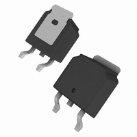
... DPAK IPAK (TO-252) (TO-251 ORDERING INFORMATION Package DPAK (TO-252) Lead (Pb)-free and Halogen-free SiHFR420A-GE3 IRFR420APbF Lead (Pb)-free SiHFR420A-E3 IRFR420A SnPb SiHFR420A Note a. See device orientation. ABSOLUTE MAXIMUM RATINGS T PARAMETER Drain-Source Voltage Gate-Source Voltage Continuous Drain Current a Pulsed Drain Current Linear Derating Factor ...

Page 2

... IRFR420A, IRFU420A, SiHFR420A, SiHFU420A Vishay Siliconix THERMAL RESISTANCE RATINGS PARAMETER Maximum Junction-to-Ambient Case-to-Sink, Flat, Greased Surface Maximum Junction-to-Case (Drain) SPECIFICATIONS °C, unless otherwise noted J PARAMETER Static Drain-Source Breakdown Voltage V Temperature Coefficient DS Gate-Source Threshold Voltage Gate-Source Leakage Zero Gate Voltage Drain Current ...

Page 3

... V , Drain-to-Source Voltage (V) DS Fig Typical Output Characteristics Document Number: 91274 S10-1135-Rev. B, 10-May-10 IRFR420A, IRFU420A, SiHFR420A, SiHFU420A 4.5V ° 0.01 10 100 ° 100 Fig Normalized On-Resistance vs. Temperature Vishay Siliconix 150 C ° ° 50V DS 20μs PULSE WIDTH 4.0 5.0 6.0 7.0 8 ...

Page 4

... IRFR420A, IRFU420A, SiHFR420A, SiHFU420A Vishay Siliconix 10000 0V MHZ C iss = rss = oss = 1000 Ciss 100 Coss 10 Crss Drain-to-Source Voltage (V) Fig Typical Capacitance vs. Drain-to-Source Voltage 2. FOR TEST CIRCUIT SEE FIGURE Total Gate Charge (nC) G Fig Typical Gate Charge vs. Gate-to-Source Voltage www.vishay.com 4 SHORTED 0.1 ...

Page 5

... Fig. 12a - Unclamped Inductive Test Circuit Document Number: 91274 S10-1135-Rev. B, 10-May-10 IRFR420A, IRFU420A, SiHFR420A, SiHFU420A 125 150 ° 0.001 0. Rectangular Pulse Duration (sec Driver + - Vishay Siliconix D.U. Pulse width ≤ 1 µs Duty factor ≤ 0.1 % Fig. 10a - Switching Time Test Circuit V ...

Page 6

... IRFR420A, IRFU420A, SiHFR420A, SiHFU420A Vishay Siliconix 300 250 200 150 100 100 Starting T , Junction Temperature ( C) J Fig. 12c - Maximum Avalanche Energy vs. Drain Current Charge Fig. 13a - Basic Gate Charge Waveform www.vishay.com 6 700 I D TOP 1.1A 1.6A BOTTOM 2.5A 650 600 550 ...

Page 7

... Note Vishay Siliconix maintains worldwide manufacturing capability. Products may be manufactured at one of several qualified locations. Reliability data for Silicon Technology and Package Reliability represent a composite of all qualified locations. For related documents such as package/tape drawings, part marking, and reliability data, see www.vishay.com/ppg?91274. Document Number: 91274 S10-1135-Rev ...

Page 8

... Vishay product could result in personal injury or death. Customers using or selling Vishay products not expressly indicated for use in such applications their own risk and agree to fully indemnify and hold Vishay and its distributors harmless from and against any and all claims, liabilities, expenses and damages arising or resulting in connection with such use or sale, including attorneys fees, even if such claim alleges that Vishay or its distributor was negligent regarding the design or manufacture of the part ...

Related keywords