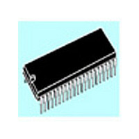
STV0042A/Z STMicroelectronics, STV0042A/Z Datasheet - Page 5

STV0042A/Z
Manufacturer Part Number
STV0042A/Z
Description
Video ICs Analog Sound/Video
Manufacturer
STMicroelectronics
Type
Audio DSPr
Datasheet
1.STV0042AZ.pdf
(37 pages)
Specifications of STV0042A/Z
Maximum Operating Temperature
+ 70 C
Package / Case
PDIP-42
Minimum Operating Temperature
0 C
Mounting Style
Through Hole
Lead Free Status / RoHS Status
Lead free / RoHS Compliant
STV0042A/Z
1.1.1
1.1.1.1 FM Demodulators
1.1.1.2 AGC Peak Detector Capacitors
1.1.1.3 Amplitude Detector Capacitors
VCR/Decoder
22 kHz to LNB
Sound Detection
A block diagram of the FM Demodulation block is shown in
Pin FMIN (pin 20) is the input to the two FM demodulators. It feeds two AGC amplifiers with a
bandwidth of at least 5 to 10 MHz. There is one amplifier for each channel. Both channels have the
same input. The AGC amplifiers have a range between 0 and +40 dB.
The input impedance (Z
input of 500 mV
phases coincide.
Pins AGCL and AGCR (pins 21 and 31, respectively) are the AGC amplifier peak detector capacitor
connections. The output current has an attack/decay ratio of 1:32. This means that the ramp-up
current is approximately 5 µA and decay current is approximately 160 µA. 11V gives maximum
gain. These pins are also driven by a circuit monitoring the voltage on pins AMPLKL and AMPLKR,
respectively.
Pins AMPLKL and AMPLKR (pins 30 and 35, respectively) are the left and right outputs of their
respective amplitude detectors. Each pin requires a capacitor and a resistor to GND. The voltage
across these pins is used to decide whether a signal is being received by the FM detector. The level
detector output drives a bit in the I²C bus detector control block. Pins AMPLKL and AMPLKR drive
also respectively pins AGCL and AGCR. For instance, when the voltage on pin AMPLKL is > (V
+ 1 V
From Tuner
From Tuner
From
BE
) it sinks current to V
PP
. This is the maximum value when all inputs are added together, when their
Figure 2: STV0042A/Z General Block Diagram
STV0042A/Z
IN
) is 5 k with a minimum input of 2 mV
& De-emphasis
REF
Demodulation
2 Channels
Processing
Reduction
B-Band
from pin AGCL in order to reduce the AGC gain.
Noise
Video
FM
2
1
2
Volume
Interface
Matrix
I²C Bus
Matrix
Audio
Video
4 x 2
&
Figure
PP
3.
per subcarrier and a maximum
2
2
Active in Standby mode
General Information
To
TV
VCR
Decoder
REF
5/37


