IRFP460APBF Vishay, IRFP460APBF Datasheet
IRFP460APBF
Specifications of IRFP460APBF
Available stocks


Related parts for IRFP460APBF


IRFP460APBF Summary of contents
Page 1
... Document Number: 91234 SMPS MOSFET HEXFET Power MOSFET V DSS 500V @ 10V GS @ 10V GS 300 (1.6mm from case ) 10 lbf•in (1.1N•m) Rds(on) max I D 0.27Ω 20A TO-247AC Max. Units 280 W 2.2 W/°C ± 3.8 V/ns - 150 °C www.vishay.com 1 ...
Page 2
... Intrinsic turn-on time is negligible (turn-on is dominated by L Conditions = 250µ 1mA D = 12A „ 250µ 0V 125° Conditions = 12A D „ = 1.0V, ƒ = 1.0MHz DS = 400V, ƒ = 1.0MHz 400V … DS Max. Units 960 Max. Units 0.45 ––– °C/W 40 Conditions „ = 20A 20A www.vishay.com 2 ...
Page 3
... Fig 4. Normalized On-Resistance VGS 15V 10V 8.0V 7.0V 6.0V 5.5V 5.0V 4.5V 4.5V 20µs PULSE WIDTH T = 150 C ° Drain-to-Source Voltage (V) DS 19A 20A V = 10V 100 120 140 160 ° Junction Temperature ( C) J Vs. Temperature www.vishay.com 100 3 ...
Page 4
... Fig 8. Maximum Safe Operating Area 19A 20A V = 400V 250V 100V DS FOR TEST CIRCUIT SEE FIGURE Total Gate Charge (nC) G Gate-to-Source Voltage OPERATION IN THIS AREA LIMITED BY R DS(on) 10us 100us 1ms ° ° = 150 C 10ms 100 1000 V , Drain-to-Source Voltage (V) DS www.vishay.com 100 10000 4 ...
Page 5
... Fig 11. Maximum Effective Transient Thermal Impedance, Junction-to-Case Document Number: 91234 Fig 10a. Switching Time Test Circuit V DS 90% 125 150 ° 10 d(on) Fig 10b. Switching Time Waveforms Notes: 1. Duty factor Peak 0.001 0. Rectangular Pulse Duration (sec ≤ 1 ≤ 0 d(off thJC C 0.1 1 www.vishay.com 5 ...
Page 6
... Starting T , Junction Temperature( C) Fig 12c. Maximum Avalanche Energy 620 600 580 560 + 540 0 Fig 12d. Typical Drain-to-Source Voltage I D TOP 8.9A 13A BOTTOM 20A 50 75 100 125 ° J Vs. Drain Current Avalanche Current (A) av Vs. Avalanche Current www.vishay.com 150 ...
Page 7
... D.U.T. V Waveform DS Re-Applied Voltage Inductor Curent Document Number: 91234 + • • ƒ • - „ • • • • P.W. Period D = Period Body Diode Forward Current di/dt Diode Recovery dv/dt Body Diode Forward Drop Ripple ≤ 5% Fig 14. For N-Channel HEXFETS + - V =10V www.vishay.com 7 ...
Page 8
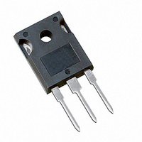
... CONFORMS TO JEDEC OUTLINE TO-247-AC. LEAD ASSIGNMENTS Hexfet IGBT LEAD ASSIGNMENTS 1 - Gate 1 - Gate 0.80 (.031 Drain 1 - GATE 2 - Collector 0.40 (.016 DRAIN 3 - Source 3 - Emitter 3 - SOURCE 4 - Drain 4 - Collector 4 - DRAIN PART NUMBER 035H 57 DAT E CODE YEAR 0 = 2000 WEEK 35 LINE H DSS TAC Fax: (310) 252-7903 11/03 www.vishay.com 8 ...
Page 9
... Except as provided in Vishay's terms and conditions of sale for such products, Vishay assumes no liability whatsoever, and disclaims any express or implied warranty, relating to sale and/or use of Vishay products including liability or warranties relating to fitness for a particular purpose, merchantability, or infringement of any patent, copyright, or other intellectual property right. ...