IRFP32N50KPBF Vishay, IRFP32N50KPBF Datasheet
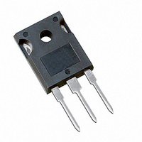
MOSFET N-CH 500V 32A TO-247AC

IRFP32N50KPBF

Manufacturer Part Number
IRFP32N50KPBF
Description
MOSFET N-CH 500V 32A TO-247AC
Manufacturer
Vishay
Type
Power MOSFETr
Datasheets

Specifications of IRFP32N50KPBF

Transistor Polarity
N-Channel
Fet Type
MOSFET N-Channel, Metal Oxide
Fet Feature
Standard
Rds On (max) @ Id, Vgs
160 mOhm @ 32A, 10V
Drain To Source Voltage (vdss)
500V
Current - Continuous Drain (id) @ 25° C
32A
Vgs(th) (max) @ Id
5V @ 250µA
Gate Charge (qg) @ Vgs
190nC @ 10V
Input Capacitance (ciss) @ Vds
5280pF @ 25V
Power - Max
460W
Mounting Type
Through Hole
Package / Case
TO-247-3 (Straight Leads), TO-247AC
Minimum Operating Temperature
- 55 C
Configuration
Single
Resistance Drain-source Rds (on)
0.16 Ohm @ 10 V
Drain-source Breakdown Voltage
500 V
Gate-source Breakdown Voltage
+/- 30 V
Continuous Drain Current
32 A
Power Dissipation
460000 mW
Maximum Operating Temperature
+ 150 C
Mounting Style
Through Hole
Continuous Drain Current Id
32A
Drain Source Voltage Vds
500V
On Resistance Rds(on)
160mohm
Rds(on) Test Voltage Vgs
10V
Threshold Voltage Vgs Typ
5V
Number Of Elements
1
Polarity
N
Channel Mode
Enhancement
Drain-source On-res
0.16Ohm
Drain-source On-volt
500V
Gate-source Voltage (max)
±30V
Drain Current (max)
32A
Output Power (max)
Not RequiredW
Frequency (max)
Not RequiredMHz
Noise Figure
Not RequireddB
Power Gain
Not RequireddB
Drain Efficiency
Not Required%
Operating Temp Range
-55C to 150C
Operating Temperature Classification
Military
Mounting
Through Hole
Pin Count
3 +Tab
Package Type
TO-247AC
Lead Free Status / RoHS Status
Lead free / RoHS Compliant
Lead Free Status / RoHS Status
Lead free / RoHS Compliant, Lead free / RoHS Compliant
Other names
*IRFP32N50KPBF

Available stocks

Company
Part Number
Manufacturer
Quantity
Price
Part Number:
IRFP32N50KPBF
Manufacturer:
IR
Quantity:
20 000
Thermal Resistance
Benefits
l
l
l
l
Applications
l
l
l
l
l
Avalanche Characteristics
Document Number: 91221
Absolute Maximum Ratings
I
I
I
P
V
dv/dt
T
T
Symbol
E
I
E
Symbol
R
R
R
D
D
AR
DM
J
STG
D
GS
AS
AR
θJC
θCS
θJA
Drive Requirement
dv/dt Ruggedness
Avalanche Voltage and Current
@ T
@ T
Switch Mode Power Supply (SMPS)
Uninterruptible Power Supply
High Speed Power Switching
Hard Switched and High Frequency
Lead-Free
Low Gate Charge Qg results in Simple
Improved Gate, Avalanche and Dynamic
Fully Characterized Capacitance and
Low R
@T
Circuits
C
C
C
= 25°C
= 100°C
= 25°C
DS(on)
Continuous Drain Current, V
Pulsed Drain Current 
Power Dissipation
Linear Derating Factor
Gate-to-Source Voltage
Peak Diode Recovery dv/dt ƒ
Operating Junction and
Storage Temperature Range
Soldering Temperature, for 10 seconds
Mounting torque, 6-32 or M3 screw
Single Pulse Avalanche Energy‚
Avalanche Current
Repetitive Avalanche Energy
Junction-to-Case
Case-to-Sink, Flat, Greased Surface
Junction-to-Ambient
(1.6mm from case )
Parameter
Parameter
Parameter
SMPS MOSFET
GS
GS
@ 10V
@ 10V
V
500V
IRFP32N50KPbF
DSS
Typ.
Typ.
0.24
–––
–––
–––
–––
–––
-55 to + 150
HEXFET Power MOSFET
Max.
130
460
± 30
300
3.7
32
20
13
R
DS(on)
0.135Ω
TO-247AC
Max.
Max.
typ.
0.26
450
–––
32
46
40
www.vishay.com
10lb*in (1.1N*m)
Units
W/°C
V/ns
°C
W
A
V
Units
Units
°C/W
32A
2/26/04
mJ
mJ
I
A
D
1

Related parts for IRFP32N50KPBF

IRFP32N50KPBF Summary of contents

Page 1

... Repetitive Avalanche Energy AR Thermal Resistance Symbol Parameter R Junction-to-Case θJC R Case-to-Sink, Flat, Greased Surface θCS R Junction-to-Ambient θJA Document Number: 91221 IRFP32N50KPbF SMPS MOSFET HEXFET Power MOSFET V DSS 500V @ 10V GS @ 10V GS - 150 Typ. ––– ––– ––– ...

Page 2

... G = 10V „ 25V DS pF ƒ = 1.0MHz, See Fig 0V 1.0V, ƒ = 1.0MHz 0V 400V, ƒ = 1.0MHz 0V 400V … Conditions MOSFET symbol showing the A integral reverse G p-n junction diode 25° 32A „ 25° 32A J F µC di/dt = 100A/µs „ DSS www.vishay.com ...

Page 3

... Fig 2. Typical Output Characteristics 3 2.5 2.0 1.5 1.0 0.5 = 50V 0 -60 -40 -20 Fig 4. Normalized On-Resistance VGS 15V 12V 10V 8.0V 7.0V 6.0V 5.5V 5.0V 20µs PULSE WIDTH Tj = 150° Drain-to-Source Voltage (V) 32A V = 10V 100 120 140 160 ° Junction Temperature ( C) J Vs. Temperature www.vishay.com 100 3 ...

Page 4

... OPERATION IN THIS AREA LIMITED 100 ° 150 Single Pulse GS 1 1.3 1.6 10 Fig 8. Maximum Safe Operating Area 32A V = 400V 250V 100V 120 160 Q , Total Gate Charge (nC) G Gate-to-Source Voltage BY R DS(on) 10us 100us 1ms ° 10ms 100 1000 V , Drain-to-Source Voltage (V) DS www.vishay.com 200 10000 4 ...

Page 5

... Fig 11. Maximum Effective Transient Thermal Impedance, Junction-to-Case Document Number: 91221 Fig 10a. Switching Time Test Circuit V DS 90% 125 150 ° 10 d(on) Fig 10b. Switching Time Waveforms Notes: 1. Duty factor Peak 0.001 0. Rectangular Pulse Duration (sec ≤ 1 ≤ 0 d(off thJC C 0.1 1 www.vishay.com 5 ...

Page 6

... Fig 13a. Gate Charge Test Circuit Document Number: 91221 I D TOP 14A 20A BOTTOM 32A 20V Fig 12c. Unclamped Inductive Test Circuit 125 150 ° Fig 12d. Unclamped Inductive Waveforms Fig 13b. Basic Gate Charge Waveform 15V DRIVER L D.U 0.01 Ω (BR)DSS Charge www.vishay.com A 6 ...

Page 7

... Inductor Curent Fig 14. For N-Channel HEXFET Document Number: 91221 + • • ƒ • - „ - • • • • P.W. Period D = Period Waveform Body Diode Forward Current di/dt Waveform Diode Recovery dv/dt Body Diode Forward Drop Ripple ≤ 5% ® Power MOSFETs + + - V =10V www.vishay.com 7 ...

Page 8

... CONTROLLING DIMENSION : INCH. 3 CONFORMS TO JEDEC OUTLINE TO-247-AC. LEAD ASSIGNMENTS Hexfet IGBT LEAD ASSIGNMENTS 1 - Gate 1 - Gate 0.80 (.031 Drain 1 - GATE 2 - Collector 0.40 (.016 DRAIN 3 - Source 3 - Emitter 3 - SOURCE 4 - Drain 4 - Collector 4 - DRAIN PART NUMBER 57 DAT E CODE YEAR 0 = 2000 WEEK 35 LINE H TAC Fax: (310) 252-7903 www.vishay.com 8 ...

Page 9

... Except as provided in Vishay's terms and conditions of sale for such products, Vishay assumes no liability whatsoever, and disclaims any express or implied warranty, relating to sale and/or use of Vishay products including liability or warranties relating to fitness for a particular purpose, merchantability, or infringement of any patent, copyright, or other intellectual property right. ...

Related keywords