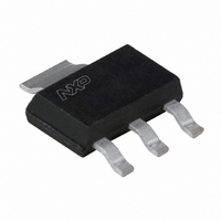
BSP130,115 NXP Semiconductors, BSP130,115 Datasheet - Page 4

BSP130,115
Manufacturer Part Number
BSP130,115
Description
MOSFET N-CH 300V 350MA SOT223
Manufacturer
NXP Semiconductors
Datasheet
1.BSP130115.pdf
(12 pages)
Specifications of BSP130,115
Package / Case
SOT-223 (3 leads + Tab), SC-73, TO-261
Mounting Type
Surface Mount
Power - Max
1.5W
Fet Type
MOSFET N-Channel, Metal Oxide
Vgs(th) (max) @ Id
2V @ 1mA
Current - Continuous Drain (id) @ 25° C
350mA
Drain To Source Voltage (vdss)
300V
Fet Feature
Logic Level Gate
Rds On (max) @ Id, Vgs
6 Ohm @ 250mA, 10V
Minimum Operating Temperature
- 55 C
Configuration
Single Dual Drain
Transistor Polarity
N-Channel
Resistance Drain-source Rds (on)
6 Ohm @ 10 V
Drain-source Breakdown Voltage
300 V
Gate-source Breakdown Voltage
+/- 20 V
Continuous Drain Current
0.35 A
Power Dissipation
1500 mW
Maximum Operating Temperature
+ 150 C
Mounting Style
SMD/SMT
Lead Free Status / RoHS Status
Lead free / RoHS Compliant
Gate Charge (qg) @ Vgs
-
Lead Free Status / Rohs Status
Lead free / RoHS Compliant
Other names
934023500115::BSP130 T/R::BSP130 T/R
Philips Semiconductors
2001 Dec 11
handbook, halfpage
handbook, halfpage
N-channel enhancement mode
vertical D-MOS transistor
P tot
(W)
1.5
0.5
2
1
0
0
10 V
0 V
Fig.2 Switching times test circuit.
Fig.4 Power derating curve.
50
50
100
V DD = 50 V
I D
150
MBB691
T j ( C)
MRC218
200
4
handbook, halfpage
handbook, halfpage
V
Fig.5
GS
(pF)
250
200
150
100
= 0; f = 1 MHz; T
INPUT
OUTPUT
C
50
0
0
Capacitance as a function of drain-source
voltage; typical values.
Fig.3 Input and output waveforms.
10 %
j
t on
= 25 C.
10
90 %
90 %
20
Product specification
V DS (V)
t off
C oss
BSP130
C iss
C rss
MLD765
MBB692
10 %
30


